|
|
|
|
|
|
PCB transmission line configurations
Application Note AP121
|
|
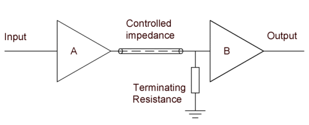
PCB traces as transmission lines Short signal transition times and high clock rates mean that today's PCB traces need to be considered as transmission lines (see Application Note AP120.) This application note briefly discusses two configurations of transmission line. Transmission lines are signal lines whose electrical characteristics must be controlled by the PCB designer. One critical parameter is the characteristic impedance of the PCB trace (that is, the ratio of voltage to current of a wave moving down the signal transmission line). In practice that means you'll have to control trace impedance when designing for digital edge speeds faster than 1ns or analog frequencies greater than 300mhz. Roughly, designers will need to consider controlled impedance boards when the electrical length of the signal line exceeds thirty per cent of the signal rise time. Matching transmission lines to device impedance The devices mounted on a PCB themselves possess characteristic impedance and the impedance of the interconnecting PCB traces must be chosen to match the characteristic impedance of the logic family in use. In order to maximise signal transfer from source (device A in the diagram) to load (device B) the trace impedance must match the output impedance of the sending device (device A) and the input impedance of the receiving device (device B). For CMOS and TTL this will be in the region of 80 to 110 ohms. If the impedance of the PCB trace connecting two devices does not match the devices' characteristic impedance, multiple reflections will occur on the signal line before the load device can settle into a new logic state. The result will probably be increased switching times or random errors in high speed digital systems. The value and tolerance of trace impedance must therefore be carefully specified by the circuit design engineer and the PCB designer. Tolerances of 5% are not uncommon for high specification applications. Single-ended transmission lines The circuit in Figure 1 is an example of a single-ended transmission line.
Figure 1 - Single-ended PCB trace The single-ended transmission line is probably the commonest way to connect two devices. In this case a single conductor connects the source of one device to the load of another device. The reference (ground) plane provides the signal return path. This is an example of an unbalanced line. The signal and return lines differ in geometry — the cross-section of the signal conductor is different from that of the return ground plane conductor. So what determines the characteristic impedance of a PCB trace? The impedance of a PCB trace will be determined by its inductive and capacitive reactance, resistance and conductance. These will be a function of the physical dimensions of the trace (e.g. trace width and thickness) and the dielectric constant of the PCB substrate material and dielectric thickness. PCB impedances will typically range from 25 to 120 ohms. In practice, a PCB transmission line typically consists of a line conductor trace, one or more reference planes and a dielectric material. The trace and plane(s) form the controlled impedance. The PCB will frequently be multi-layer in fabrication and the controlled impedance can be constructed in several ways. However, whichever method is used the value of the impedance will be determined by its physical construction and electrical characteristics of the dielectric material:
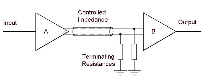
Differential transmission lines Controlledimpedance PCBs are usually produced using microstrip or stripline transmission lines in single-ended (unbalanced) or differential (balanced) configurations. The differential mode of operation is shown in Figure 2.
Figure 2 – Differential PCB trace The differential configuration is used when better noise immunity and improved timing are required in critical applications. This configuration is an example of a balanced line — the signal and return paths have similar geometry. The lines are driven as a pair with one line transmitting a signal waveform of the opposite polarity to the other. Fields generated in the two lines will tend to cancel each other, so EMI and RFI will be lower than with the unbalanced line and problems with external noise are reduced. |