|
|
|
|
|
|
Testing and modelling impedance of differential pairs without ground
Application Note AP153
|
|
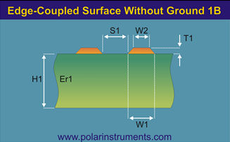
(Applies to Si8000m/Si9000e v16.03 onwards) Scope This application note refers to testing and modelling balanced differential pairs where there are no reference planes. If your application is on board test of differential traces where direct access to the ground plane is difficult or impossible see the CITS880s controlled impedance test system (2015 editions onwards) which supports groundless differential probes. Differential pairs without ground planes The structure pictured below is defined as an edge coupled differential pair without ground plane. From a modelling standpoint the structure is like a paired wire transmission line. However, you may ask, "As this is a differential structure, how you should test the impedance?"
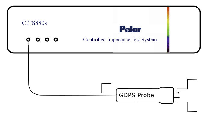
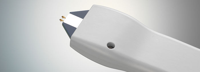
Edge coupled differential pair without ground plane Testing In a structure as pictured above all the signal current flows out through one conductor and the return comes back through the other. With a signal of equal positive and negative going potential a virtual ground exists midway between the two traces, similar to a twisted pair. G-Series groundless differential probes To test such structures Polar produces a range of groundless differential probes. Polar GDPS (groundless diferential) probes are supported by the Polar CITS880s and provide a measurement solution for situations where there is no physical access to the ground plane, or where a ground plane is not present, i.e. a balanced line with equal width signal and return path.
Polar CIT880s with GDPS probe GDPS probes convert the single ended signal from the CITS880s to a differential signal that is applied to the coupon under test. The reflected signals from the coupon are converted back to single ended as they return through the probe to the CITS880s.
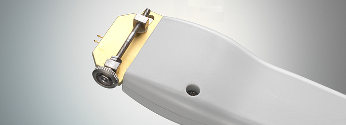
Polar's proprietary probe technology thus enables groundless differential probes to be connected – with a single coaxial cable – reducing operator fatigue and cost of ownership. V-Series precision variable pitch probes Precision variable pitch probes are available as groundless differential probes as well as single ended alternatives.
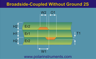
Precision adjustment is ideal for situations where the boards you test are in low volumes and have a high variety of footprints. Yes, but I need to model this structure... The Polar Si8000m and Si9000e field solvers include a range of controlled impedance structures for modelling differentials without grounds (no reference planes.) Example structures are shown below. The Si8000m and Si9000e Differential Without Ground Structures models are primarily aimed at low layer count stackups commonly used in the flex market and can prove useful when no reference planes exist within the stackup. 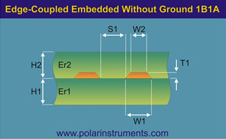
|
|
If you have found this note useful you may also find Application Note AP151 of interest. AP151 discusses how copper thickness influences the impedance of the above structure. |