|
|
|
|
|
|
Ground plane thickness in Si9000 frequency dependent calculations
Application Note AP189
|
|||
|
Modelling skin depth in ground planes with the Si9000e This application note describes how the Si9000 PCB Transmission Line Field Solver fully takes into consideration power plane thickness in frequency dependent calculations.
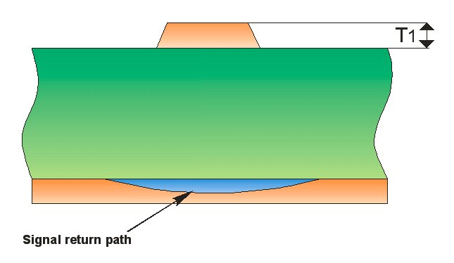
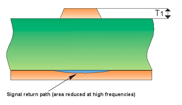
Signal return path in the reference plane The diagram above shows a surface microstrip structure; the blue area indicates the (simplified) signal return path field in the reference plane. The signal return path is fully accounted for within the Si9000's Boundary Element Method calculation. The area that the field occupies in both the trace and the associated reference plane is largely determined by the frequency for which the calculation is done. This is calculated and presented to the user in the Si9000 as the Skin Depth. As the signal frequency increases the area that both the signal and ground return occupy is reduced and both signal and return losses increase. At higher frequencies the return path area will reduce as shown below (simplified).
The signal return path at low frequencies From the above we can also conclude that skin depth will increase as the frequency is reduced. So what happens when the signal frequency is low enough to cause the skin depth to be greater than the thickness of the power plane? In practice this situation is seldom achieved as the signal trace encounters a similar skin depth issue; however the trace has skin depth reducing its available area simultaneously from the top and the bottom of the trace. (For a surface microstrip, the current in the signal trace will be concentrated in the lower portion of the trace; in a stripline structure, current in the signal trace will be concentrated in the upper and lower portions of the trace.) The sides of the trace are similarly affected, but for simplicity we assume that trace width is significantly greater than trace height. |
|||