PCB test signature differences device vendor differences, or a genuine fault?
|
||
| Printer Friendly Version | |
|
Application Note
205 PCB test signature differences device vendor differences, or a genuine fault? |
| Printer Friendly Version | |
| Using
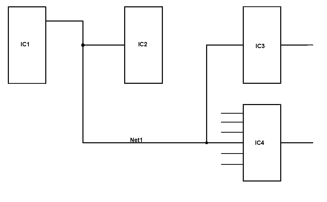
Nodal Impedance techniques to locate faults on a net Consider the circuit below. Net1 connects the devices as shown. |
|
|
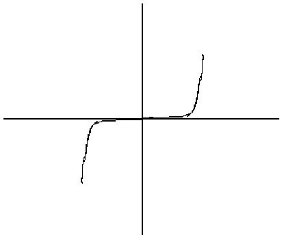
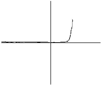
Comparing bus signatures In this example other net signatures
look correct (see Fig 2), but the signature on Net1 and the signatures
all the other pins on IC4 appear as in Fig 3. |
|
|
|
The signatures on the good nets are typical of many data bus signatures and portray the behaviour of the device input protection diode circuitry. |
|
|
On this board, the signature on the faulty Net1 shows significant differences from the reference signature. All the pins on this device (IC4) display similarly faulty signatures. |
| So
why the difference between the signatures? Look at the way signatures
are created.
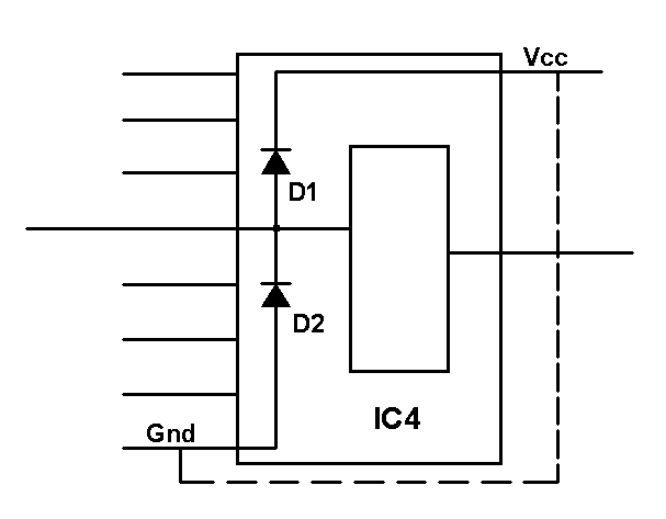
Polar's nodal impedance testers apply a sinusoidal waveform across a net under test and COM (usually ground) and display a graph of applied voltage versus resultant current (the net's signature). In digital circuits, you're actually applying the test voltage to the diode protection circuits of the digital IC. Consider IC4 below (Fig
4). The diagram shows a typical (simplified) protection circuit
comprising diodes D1 and D2, designed to protect the IC against
voltage swings below ground and above Vcc (only one line is shown but
all lines would have similar protection). |
|
|
|
Device
protection circuits Looking inside IC4 note the typical two-diode protection circuit, designed to guard against signal voltage swings outside the VccGnd range. |
| When
testing boards with digital ICs it's common practice to connect the
COM line to a convenient ground point on the board under test and also
to the Vcc line, effectively shorting Vcc and ground. This can help
improve the stability of signatures by removing the effects of
charging/discharging the device decoupling capacitors . (See App Note
103.)
With Vcc and Gnd shorted, the applied sine wave will forward bias diode D1 and cause current to flow through D1 on the positive half cycle and do the same for D2 on the negative half cycle (the voltage applied by the tester will be sufficient on most ranges to cause both diodes to conduct). The result is the characteristic bus line signature (Fig 2). All pins on a digital IC will include similar protection circuitry so all should exhibit similar signatures. In this case the faulty signature (Fig 3) appeared on all of IC4's lines, so the faulty signature revealed that each protection circuit's D2 was not conducting. This could be caused by a faulty or wrong device or it may indicate differences in diode protection configuration between device vendors. While checking the signatures of this device with other devices from the same vendor (i.e. the same device on other boards), IC4 on other boards displayed the correct signature (Fig 2), ruling out device vendor differences.The faulty signatures showed that no return path existed for current in any of the D2s. The line common to all D2s is the ground line. Checking the ground line showed up an unsoldered pin (open circuit ground). As you can see, the fault would be difficult to detect using conventional methods, and probing the pin itself would have temporarily rectified the fault. By using net impedance analysis the fault could be approached and detected using logical detective techniques. |
|
Polar Instruments Ltd www.polarinstruments.com Tel: +44 1481 253081 Fax: +44 1481 252476 © Polar Instruments 2002 |
 |
| © Polar Instruments 2002. Polar Instruments pursues a policy of continuous improvement. The specifications in this document may therefore be changed without notice. All trademarks recognised. | |