| RIE loss measurement method and PCB manufacture | |||
Note: The RIE (Root Impulse Energy) loss measurement technique is a loss measurement technology that was explored but is no longer supported by Polar Instruments – this note is included in the Polar Signal Integrity Application Note series for historical interest. RIE has been superseded by the SET2DIL methodology (see AP8168 – PCB fabrication techniques for lossy transmission lines) as used in Polar's Atlas PCB lossy line test system.
The RIE loss /
attenuation measurement
method and PCB manufacture
What is RIE?
RIE (Root Impulse Energy) testing is one of 4 PCB
material loss (attenuation) measurement methods which will be included in IPC-TM-650 Method
2.5.5.12 (Time Domain Loss) when it is finally published
in mid-2009. This test method is aimed at the manufacturing shop floor to provide a relatively
straight-forward method of monitoring the high frequency performance of
PCBs to ensure they stay within an acceptable loss budget.
What is Loss?
Signals propagating through a system lose strength while encountering
both natural and manmade obstacles; signal loss is
generally measured in decibels. If a signal enters one end of a PCB
trace and is only half the size at the other end then that trace has significant loss.
If losses are too great not enough signal will get to the other end to make
the system
work reliably. Conversely, one might also infer that too little loss indicates that you
may have used materials which are too high performance and therefore too costly in the stack up.
At lower frequencies (i.e. at frequencies up to about
1GHz) loss was not seen as a
major concern. However, loss is now becoming a factor in PCB designs because of changing technology
(for example, very high speed multi-gigabit-per-second serial buses)
which is running at ever higher speeds. At data
transmission rates above about 5Gbps loss matters.
Doesn't the controlled impedance test check for this already?
No, controlled impedance test and RIE testing are complementary but do not test the same things.
At these very high speeds you need both measurement
techniques — you can't measure loss without confirming the controlled impedance performance first.
What does an RIE test involve?
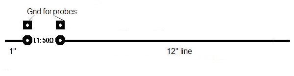
First, it needs a special coupon on the panel. The coupon
typically includes a short reference trace and a longer
measurement, or test, trace. In the 50 Ohm example below (not
drawn to scale) the reference trace is 1" in
length, the measurement trace 12".
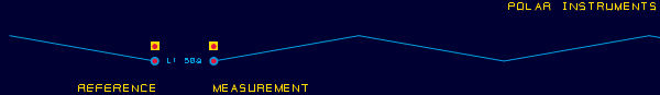
In practice, the measurement trace will be aligned so as to avoid the trace running with the warp or weft of the material, thus minimizing the effect of dielectric variation sometimes caused by trace alignment with the fibre weave. A typical zigzag measurement trace routing is shown in the sample coupon below. The test coupon was generated using the Polar Instruments' CGen Coupon Generator.
Using Polar's CGen Coupon Generator the PCB designer or fabricator can create test coupons from scratch or take impedance controlled stackup information directly from Speedstack PCB or Speedstack Si and generate the appropriate impedance test coupon containing all the required PCB controlled impedance transmission line structures.
The coupon is tested with a TDR tester in much the same way as for controlled impedance.
The RIE test does not replace conventional impedance control techniques that are currently in
use; in fact one of the tests conducted is designed to make sure the coupon is
a 50 Ohms impedance. The TDR waveforms are sent as a data file to the computer and processed using complex maths to analyse and extract the changes which have occurred to the pulse as it
travelled down the
coupon (and back). The final outcome is a number which is a figure of merit for the board related to its loss characteristics. Use different material in the stack up and you will get a different
number; a bigger number means more loss.
Is RIE testing suitable for the production environment?
Tests conducted by Polar
and Intel show that RIE testing is a practical and achievable test method; it is easily deployed and offers,
for example, repeatable, reliable discrimination between PCBs fabricated with a range of varying base material loss characteristics.
At this time, however, there are no standards for loss in the
way the industry has airlines for impedance standards. Airlines can be calibrated to national standards and are recognised as a reliable point of reference. Work is under way to try to establish
standards for loss. However, until such standards are
widely available OEMS will need to establish their own
internal standards and share these with their
fabrication partners to ensure correlation between
sites.
References:
Towards a PCB Production Floor Metric for Go/No Go
Testing of Lossy High-Speed Transmission Lines Brandon
Gore, Richard Mellitz, Jeff Loyer, Intel
Martyn Gaudion, Jean
Burnikell, Paul Carré, Polar Instruments
IPC, 2008
(U.S. Best paper at the 2008 IPC Printed Circuits Expo®
and APEX® and the Designers' Summit)