|
|
|
|
|
|
Calculating differential and coplanar impedance on FR4
Application Note AP125
|
|
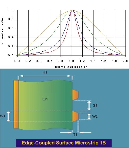
How the composite structure of FR4 effects the prediction of impedance. FR4 is a composite material, in most cases its a good approximation to assume a dielectric constant Er of 4.2, however research into the prediction of impedance of edge coupled differential and co planar structures has shown for the best results you need to take into account the composite structure of the material The two main constituents of FR4 are glass with an Er of around 6 and resin with a dielectric constant of around 3. Typically manufacturers quote a dielectric constant for the composite "c" stage material of around 4.2. The figure below shows the distribution of electric field in an edge coupled surface microstrip structure. The narrow distribution shows the field in a structure where the differential pair is closely spaced, the broader curves show how the field spreads out as the separation of the traces (S1) is increased. The actual structure is shown underneath and rotated through 90 degrees to help visualise the field distribution:
|
|
Remember that FR4 boards are built of layers of core and prepreg material. If a glass layer is close to the surface and the traces are closely spaced (the red line on the graph) the field will experience an Er value that is closer to that of glass than resin. On inner layers the space between the two traces will fill with resin and a lower effective dielectric constant will result.
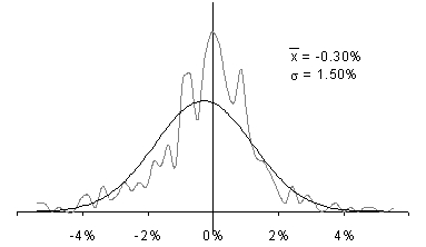
The curve below is taken from actual data used to verify Polar's field solving impedance calculator Si8000. The overall distribution of error fits the normal curve, but the analysis of the 3 peaks points to the errors from the material properties described above; data were based on 1200 samples from 3 independent PCB vendors Impedance verified against traceable reference air lines. |
|
|
Propagation Velocity consideration If propagation time is critical remember:
The variations in effective Er will alter propagation velocity and may need to be taken into consideration in addition to impedance on critical designs. In summary, you need to take into account the non-ideal electrical properties of substrates especially when designing edge coupled differential structures and coplanar designs. It helps to have a good working relationship between PCB designers and the board fabricators to achieve the highest possible yields. Source: Calculation of the Differential Impedance of Tracks on FR4 Substrates Dr J. Alan Staniforth, Gary Rich, Chris Gregg |