|
|
|
|
|
|
Signal integrity effects of vias, stubs and minimizing their visibility
Application Note AP8166
|
|
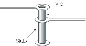
Note: This note describes single ended vias. Si8000m and Si9000e now also support models for differential vias – see the associated Application Note, Modelling plated through hole vias Many of our PCB design customers ask us about modelling plated through hole (PTH) vias with respect to impedance and signal integrity, recognizing the need to present to a signal a constant impedance as it propagates between devices. Full via modelling requires the sophistication of tools such as 3D full-wave simulators; however, there are several simple steps that can be taken to mitigate the effects of vias that are cost and time effective and that should be considered before resorting to a 3D solver. In addition, it's sometimes overlooked that, from a signal integrity standpoint, unconnected via stubs have a far larger effect on the signal than the geometry of the via itself. This application note explains how to check if, at your desired bit rate or operating frequency, you need to take steps to reduce or remove the effects of via stubs. Some of the conclusions you will discover in the text are quite surprising and often counter intuitive... Nets and signal trace discontinuities Electrical signals propagate through a PCB system via the metalwork traces (usually copper) connecting devices to each other. Each single piece of copper that connects devices together is referred to as a net. The net trace will exhibit some characteristic impedance determined, in part, by its cross section and geometry. Provided the impedance seen by the signal remains the same the signal propagates down the net undistorted. A change in impedance will cause a portion of the signal to be reflected at the point of change; such reflections represent distortion of the signal. A feature that causes a change in impedance is referred to as a discontinuity; for example, a discontinuity can result from an open circuit at the end of a net, a change in trace width, a branch or stub on the net – or a via carrying the net to a different layer – see Figure 1.
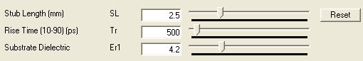
Figure 1 Via modelling A via presents a short section of change of geometry to the net and can appear as a capacitive and/or an inductive discontinuity, resulting in reflections and some degradation of the signal as it travels through the via. In many cases, however, the effects of the discontinuity will be reflections that are, for practical purposes, negligible, especially if the electrical length of the via is short compared with the risetime of the signal. In general, vias should be made such that the via delay is significantly shorter than the signal risetime. If the signal risetime approaches the via delay it will be necessary to model the via behaviour accurately (with, say, a 3D field solver), but the performance of a digital signal passing through such a via would probably not be good in any case. Stubs In Figure 1 above the via has been drilled through the board; current only travels through the via portion between the two traces; the via will typically be very short compared with the overall length of the traces. Below this portion, however, the unused stub, a conductive portion of the via not connected in series with the circuit, presents itself as an unterminated transmission line with significant signal degradation around its resonant frequency (determined by the quarter wavelength of the structure.) The longer the stub, the larger the impedance discontinuity and consequent loss to the signal path. In general, a stub presents significantly more signal degradation than the via itself. Back-drilling Stubs generally serve no useful purpose in a circuit so are often removed by back-drilling. Back-drilling (where the undesired conductive plating in the stub section of the via is removed using a drill bit slightly larger in diameter than the drill bit used to create the original via hole) can provide significant improvements, especially if the stub is long. Back-drilling can improve impedance matching and reduce resonance with consequent reduced signal attenuation, reduce EMI/EMC radiation and reduce crosstalk between vias. A full analysis of stub behaviour is possible with 3D full-wave simulation but a rule of thumb commonly employed by many signal integrity engineers is simply to (bypass the time-consuming analysis and) make the stub length as short as possible. Si9000 Via Stub Check The Si9000 incorporates a Via Stub check that provides a simple color coded go/no go check on the potential for signal distortion of a via stub. The effects of the stub will increase as the stub length and Er increase and the signal rise time reduces.
Simple interactive controls allow rapid analysis of the potential effects of a via's stub for different values of stub length, signal risetime and dielectric constant.
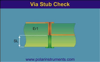
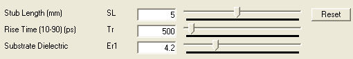
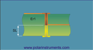
Figure 2 - 2.5mm stub Use the Si9000 screen controls to specify values for stub length, signal rise time and Er1, the substrate dielectric constant; the Si9000 calculates the results of the combination of the three factors and changes the stub color to reflect the electrical significance of the stub. In Figure 2 the Si9000 determines that the effects of the 2.5mm stub in the structure above can be ignored for signal rise times longer than 500ps. In the example below we move the stub length control to 5 to model the effects of a stub length of 5mm.
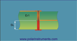
Figure 3 - 5mm stub The 5mm stub shown in Figure 3 above may result in significant signal distortion
Figure 4 - 7.5mm stub The model in Figure 4 above shows that for this structure a stub length of 7.5mm is likely to cause serious signal degradation. There are several techniques commonly employed to minimise the effects of via stubs in addition to the back-drilling process discussed above. Polar Instruments will be happy to discuss issues relating to via stubs on boards with customers with Polarcare contracts. Contact Polarcare with your PolarCare number. |