|
|
|
|
|
|
Documenting specialized pcb stackups
Application Note AP524
|
|
Using the Speedstack HDI Navigator to document pcb stackup with coated and uncoated areas Question: Answer:
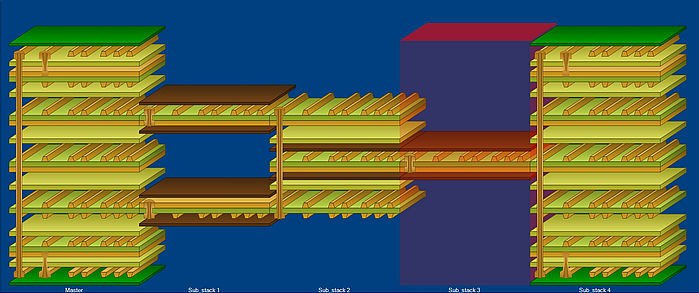
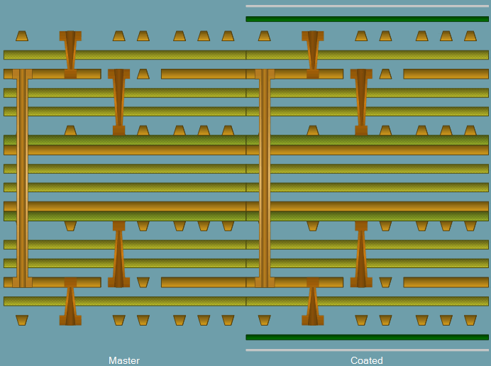
This note discusses how the Speedstack HDI Navigator can document a PCB stackup where the board includes areas that are coated with photoresist and surface traces that remain exposed. First, consider each finished sub-stack in Speedstack HDI:
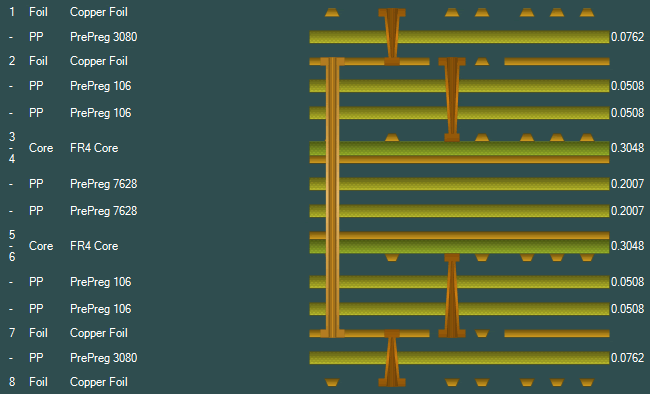
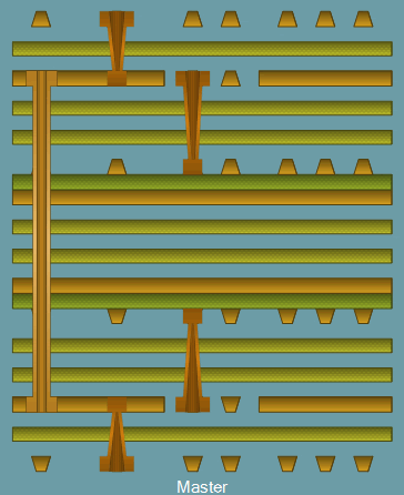
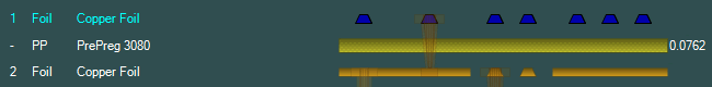
Start by creating the uncoated pcb stackup (the Master stack) in the Stack Editor, then press F4 to open the Speedstack HDI Navigator:
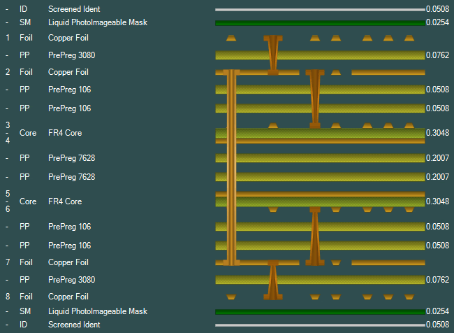
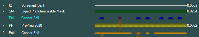
This "Master" stack represents the uncoated area; right click the Navigator and use the Addstack command to add a copy of the Master and name it "Coated". Click the new stack and return to the Stack Editor to add the photoresist and ident layers – the Navigator should display both areas as separate stacks (below).
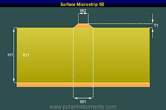
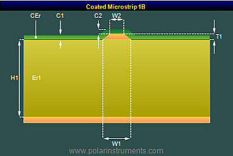
Including controlled impedance structures This example creates controlled impedance structures in both coated and uncoated areas: the uncoated areas use Surface Microstrip structures and in the coated areas Coated Microstrip structures, shown in Speedstack HDI's controlled impedance tab pane below. |
|
| Using goal seek to calculate trace widths Use Speedstack HDI's goal seeking facility to arrive at the trace widths for the two structures:
Speedstack HDI Navigator opens up not only the
capability of documenting flex-rigid stacks but also allows
you to document specialized pcb stackups. In the above example our
customer needed to produce a board which had areas
intentionally free from resist on the finished board. This
application of Speedstack HDI would be equally applicable should
a fabricator wish to predict the impedance of surface traces
on a part finished board prior to the application of resist. |