|
|
|
|
|
|
Guidance notes for using hatch plane grounds on PCB transmission lines
Application Note AP534
|
Si8000m / Si9000e / Speedstack hatch plane / mesh module Flex and flex rigid PCB fabricators have long needed a practical method of predicting the impedance of stripline and microstrip PCB traces when crosshatching (or meshed) return paths are deployed rather than the solid copper return paths of traditional rigid PCBs. Modelling impedance on traces with hatch plane grounds The shortcomings of crosshatch or mesh as a high frequency return path with all the implications of lengthened return path, etc., are well understood; however, the use of crosshatched planes on flex and flexrigid PCBs has proved a practical method of keeping controlled impedance traces at wider, more manufacturable dimensions while also achieving the desired flexibility of the assembly. Crosshatching is also deployed to keep impedance controlled line widths at reasonably manufacturable geometries – for example, on interposer boards. There are a few rules that we recommend users abide by when using the crosshatch configuration of the Si8000m and Si9000e field solvers and Speedstack PCB Stackup Builder. Crosshatch is a ‘non-ideal’ return path and is difficult to model accurately. The order of preference in the choice of reference planes is
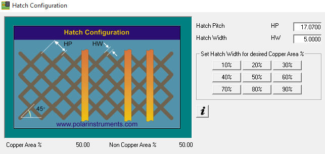
With the above in mind we recommend that users lay out the traces / crosshatch pattern as detailed in the Hatch Configuration diagram shown within the Si8000m / Si9000e or Speedstack.
Users are recommended to employ the following guidelines:
For reference, Advanced Signal Integrity for High Speed Digital Designs (Hall & Heck) includes a section on non-ideal return paths (page 422 et seq.) See Polar recommended signal integrity reading – Application Note AP194 Notes: Please note: these notes are provided as guidance – professional advice from a high speed flexible circuits Si specialist should be sought in case of doubt. The guidelines above are based on the assumption that the mesh is poured in an even line to space ratio (some purists may add the mesh at the CAD rather than the CAM stage to attempt to get the best control over registration.) However, the nature of flex base materials themselves limits the precise relation of the trace to the cross-hatch pattern. Layer registration will rarely be better than 50 microns. This can mean that the impedance of a trace traversing a hatch region can vary by ±8% from nominal, based on the relative position of the trace to the copper pattern; you might like to think of this as an exaggerated effect, similar to that which is seen with fiber weave on glass reinforced base materials. More tightly coupled differential pairs are used to mitigate the fact that registration on flexible circuits is far more challenging than on rigid. i.e. if most of the Zdiff is from coupling between signal lines rather than from signal to ground the effects of poor registration are minimised. The inherent poor registration will place further restraints on cutoff frequency if loosely coupled differential traces are used. The structures images show the limit of what is taken into account when using hatch planes – they only model to the hatch plane and not beyond it. The results will generally be found acceptable when using the models on flex as the layer counts are low and the hatch pattern is usually the bottom layer on a two layer design. However, if hatch planes are employed where other copper layers exist beyond the hatch these other layers are not taken into account with the above model. For high-speed signals consider only solid reference planes; cross hatched planes should only be considered as suitable for EMI shielding – not as a reference plane for high-speed signals. Cross-hatch copper pours should only be considered for use on flexible circuits. We recommend a copper to gap ratio of 1:1 – this will allow flexibility of the material and also provide EMI shielding for the traces. |