|
|
|
|
|
|
Overriding Speedstack library derived dielectric constant values
Application Note AP535
|
|
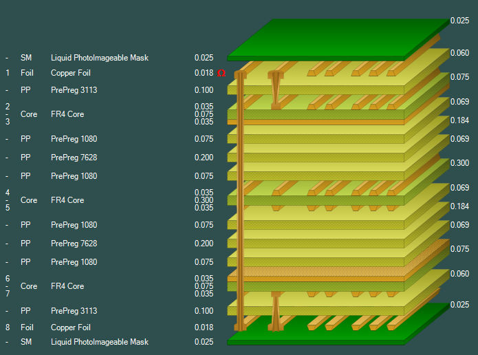
Overriding Speedstack library derived dielectric constant values Polar recommends that in 99% of situations it is best to employ the library derived dielectric constant values when adding impedance structures in Speedstack – not least because this means that all impedances will automatically be recalculated when a stack material is exchanged for another. However, recognising that life is always not so simple Speedstack 13:06 and onward offers the end user the ability to override the library derived Er on a per structure basis. Each user may have their own reason for doing this and the following note shows you how. (You will also note that the user can also select to override other parameters such as copper or coating thickness and, as PCB manufacturing technology is always changing and adapting, this ability to override selected parameters allows you to use Speedstack to document the broadest range of PCB fabrication technologies.) The relative permittivity, Er, of materials such as FR-4 varies with frequency. It may be desirable for some applications to allow Speedstack to accept different values of Er within a single material layer. A designer may want, for example, to adjust the dielectric constant value based on the frequency of the signal for different structures using the same material. Adding structures with different Er values This note will demonstrate adding four structures to a material layer then changing the Er of each structure independently of the others and using the goal seeking features of the Si8000m/Si9000e to rebuild and recalculate each structure for its target impedance. Consider the stack below.
The stack requires four structures on Layer 1 each with a different value of Er. Click the Controlled Impedance tab and the Add New Structure button
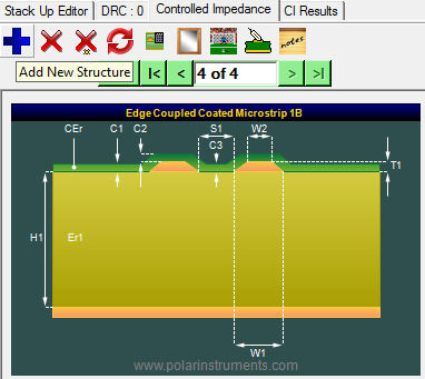
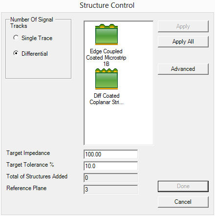
From the Structure Control dialog choose Edge-Coupled Microstrip 1B, specify a Target Impedance of 100 ohms, click Apply.
Repeat for the second structure: choose a Coated Microstrip 1B with a target impedance of 75 Ohms, then add two more edge coupled microstrips with 100 ohms as target impedance; click Done to confirm. Step through the structures using the structure navigation controls.
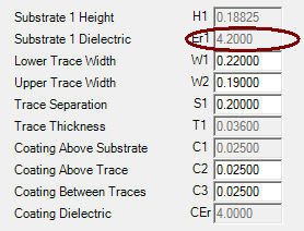
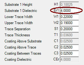
Note the value of Er – it will initially be derived from the material and thus be the same for all the structures on this layer (Note: This field will be on a grey background unless the Rebuild and Calculate Structures Substrate Dielectric (Er n) option is unchecked).
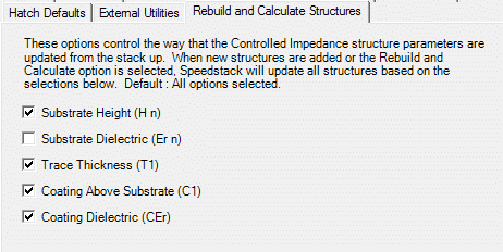
The Rebuild and Calculate Structures (Speedstack v 13.06 and later) allows the designer to specify which parameters are included when controlled impedance structures are recalculated after modifying the stack. Choose Tools|Options|Rebuild and Calculate Structures. Uncheck the Substrate Dielectric (Er n) – this will allow the value of Er to be specfied for each structure. Other parameters will be updated from the material. Click Apply.
Now you can change the value of Er for each structure – its value will not change during stack rebuilds.
Goal seeking for the target impedance Speedstack's Goal Seek allows you to change the value of Er for each structure on the layer and goal seek for the target impedance by changing, for example, trace widths, separation or dielectric height. With the new value of Er for the first structure click the Goal Seek icon:
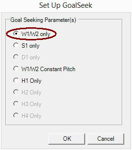
Choose the goal seeking parameters – goal seek on trace width:
The structure is rebuilt and recalculated for its target impedance. Repeat the goal seek process for each of the four structures, applying the new values for Er as appropriate for each structure; step through the structures to verify the results. Transferring layer dimensions between Speedstack and the field solver For more detailed goal seeking and sensitivity analysis the Speedstack Stackup Builder is integrated with the Si8000m/Si9000e Controlled Impedance Field Solvers. You can therefore transfer Stackup layer dimensions to the Field Solver, solve for stackup parameters to produce the target impedance then transfer the solved dimensions back to Speedstack. The structure can then be rebuilt with the new dimensions. Ensure the Field Solver is running and that its units match the Speedstack units.
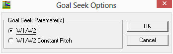
Click the To Field Solver button; use the corresponding field solver buttons to paste the values into the field solver and then solve for the target impedance by varying the trace width.
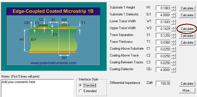
Click Upper Trace Width|Calculate and choose the W1/W2 goal seek option
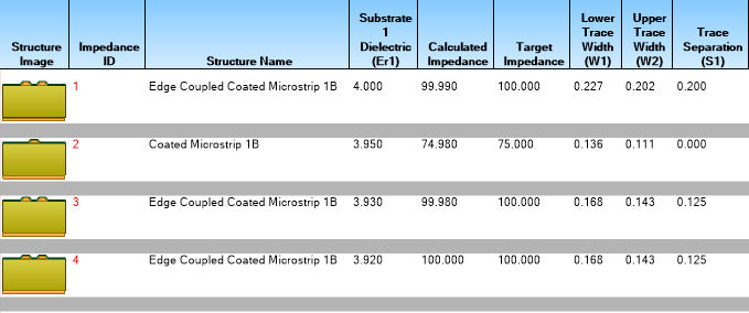
Return the values to Speedstack and rebuild/recalculate. Displaying results Repeat the process for each of the four structures, applying the new values for Er as appropriate for each structure; step through the structures to verify the results. Use Speedstack's Technical Report to display the resulting structures (below).
You will note that the resulting impedance varies as the square root of Er so the change in Er does not make a significant difference to the calculated impedance. |