|
|
|
|
|
| View equipotential lines with the EPD100 PCB track equipotential viewer | |
|
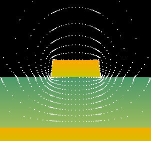
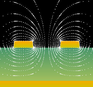
Educational tool displays equipotential lines around PCB transmission lines This free educational utility is a 2d boundary element method field solver. It allows you to view the equipotential lines around a transmission line. By seeing where the lines are densest you can view the areas of strongest field and better understand which areas of a structure have a greater effect on impedance. |
|
|
The EPD100 can plot equipotentials on both single ended microstrips and edge-coupled surface microstrips. Visualize track equipotential (below) |
|
|
|
|
|
The equipotential on the edge-coupled lines may be plotted when the lines are driven in both odd mode and even mode (more on odd and even mode.) (If you need to calculate PCB Impedance, please look at the Si8000m and Si9000e controlled impedance design pages) |
|
|
Request an installer and license: |
|
| Related information: | |
|
Calculating impedance using the Si8000 field solver: |
|
|
Design and document PCB layer stackup / buildup: |
|
|
Graph frequency dependent losses with the Si9000 field solver: |
|