
Testing Controlled
Impedance Boards
with Test Coupons
|
||
| Printer Friendly Version | |
|
Application Note 124
Testing Controlled
Impedance Boards |
| Printer Friendly Version |
| Using
test coupons to test controlled impedance boards
The accuracy of a controlled impedance trace on a PCB is usually critical to the correct performance of the PCB. We've seen from earlier application notes that the impedance of a trace depends on a number of factors, including the dimensions of the trace (i.e. trace width and thickness) and thickness and dielectric constant of the laminate and pre-preg material. It's common practice for board manufacturers to check controlled impedance build integrity initially by building engineering lots to verify copper weight, line widths and dielectric thickness and constant before beginning volume production. Even in production it's common to perform 100% controlled impedance testing on controlled impedance boards (in fact 100% controlled impedance testing will probably be part of the acceptance criteria for the board). Testing problems in practice When testing a controlled impedance PCB, however, you'll frequently run into practical difficulties. For example, it's not uncommon for a controlled impedance trace to be inaccessible for verification. Although it may be possible to add extra pads and vias to test the trace doing so will affect the performance of the trace and will occupy valuable board space. Other problems may crop up in testing:
To obviate some of these difficulties, testing is normally performed, not on the board itself, but on a test coupon manufactured at the same time and on the same panel as the PCB. Test coupons Test coupons are typically small PCBs approximately 200x30mm with exactly the same layer and trace construction as the main PCB. For example, a coupon will include traces of the same line width and copper weight on the same layer as the controlled impedances on the main PCB. The coupon will be located so as to represent actual board conditions for plating, etching and lamination. It's common practice to fabricate one coupon at each end of a board panel to verify consistency of performance across the whole panel At the time the artwork is produced, the same aperture code used for the controlled impedance traces is used to produce the test traces on the coupon. The coupon is fabricated at the same time as the main PCB so the coupon will exhibit the same impedance as the PCB. The impedance of a trace is dependent upon all the PCB's dimensions and electrical properties so the use of coupons for testing is an accurate and reliable test for manufacturing quality and consistency. |
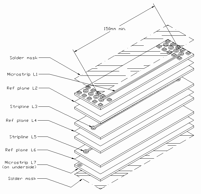 |
| Exploded
diagram of test coupon The diagram illustrates a test coupon for a board containing two microstrip traces and two stripline traces. The square pads on the surface identify the reference points for the power and ground planes. The reference planes will normally be connected to each other using plated through hole vias and brought out to the square pads. The two microstrip traces are formed by L1 and its reference plane L2, and L7 and its reference plane L6 (on the surfaces of the upper and lower layers). The two stripline traces are formed by L3, sandwiched between reference planes L2 and L4 and L5, sandwiched between reference planes L4 and L6. The coupon layers are shown on profile below. |
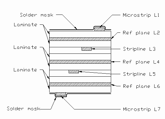 |
| Profile
of controlled impedance layers in test coupon The coupon will use the same solder mask requirements as the board. The pattern of conductors on the coupon will be designed to reproduce conditions on the board. For example, if conductors on the board are routed orthogonally a similar pattern of crossovers is used on the coupon |
Polar Instruments Ltd Garenne
Park, St Sampson, Guernsey, Channel Islands GY2 4AF, UK Tel: +44 (0) 1481 253081 Fax: +44 (0) 1481 252476 © Polar Instruments |
 |
| © Polar Instruments. Polar Instruments pursues a policy of continuous improvement. The specifications in this document may therefore be changed without notice. All trademarks recognised. | |