|
|
|
|
|
|
Pictorial representation of the proximity effect of a ground plane
Application Note AP174
|
|
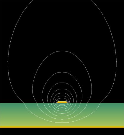
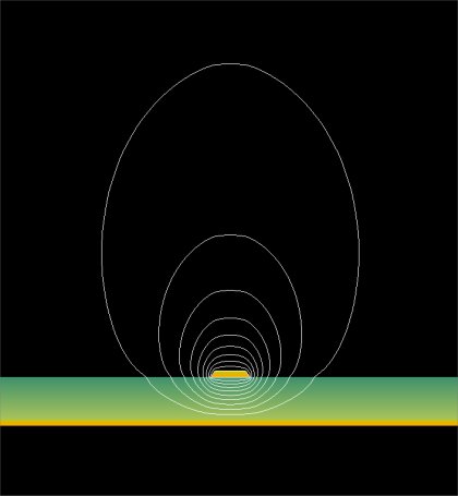
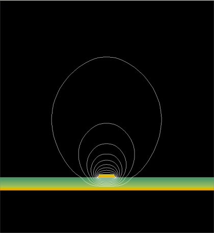
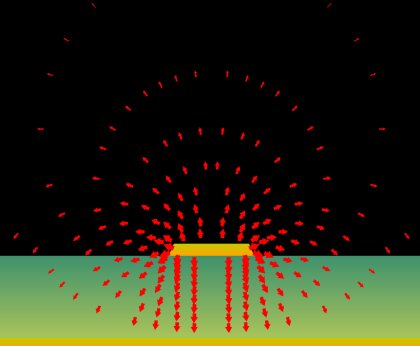
Crosstalk If PCB traces are routed closely together the signals on those traces can interfere with each other. This effect is known as crosstalk. The magnitude of the crosstalk on an adjacent trace is directly controlled by the interference of an adjacent electric field. Minimising the overlap of electric fields will minimise crosstalk and ensure maximum signal integrity. The proximity of a ground plane to the signal trace can significantly reduce the area of influence projected around a trace. Surface microstrip examples The examples in this note are for single ended surface microstrip and stripline structures. In the surface microstrip structure the electric field and the voltage equipotential lines spread out further in the air (with its lower dielectric constant) than in the underlying substrate. The three diagrams show how the electric field area associated with a trace can be significantly reduced by decreasing the height of the underlying substrate and bringing the ground plane closer to the trace. The following three diagrams show ten equipotential contours plotted at equal voltage spacing, i.e. assuming the trace is at +1V, the contours are 0.1V apart.
Fig 1:Distribution of field in dielectric and air
Fig 2: Distribution of field in dielectric and air
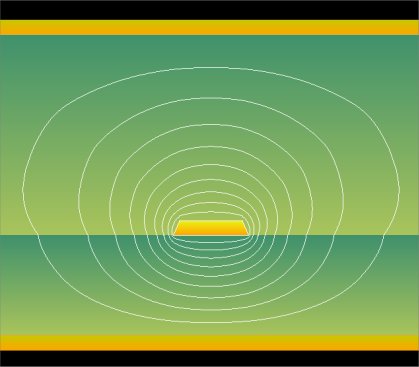
Fig 3: Distribution of field in dielectric and air The diagrams below show the equipotential voltage distribution for a single ended stripline structure over a wide variation of Er values. The voltage distribution is constrained by the presence of the ground plane above and below.
Fig 4:Equipotential distribution in multiple dielectric structure:
Fig 5:Equipotential distribution in multiple dielectric structure: There is no significant change in the potential distribution between the two structures. Any change caused by the difference in the dielectric is far outweighed by the proximity of the ground plane. An alternative view of this same situation can be seen by examining the electric field strength.
Illustration of field strength in single dielectric surface microstrip structure: In the above diagram, the strength of the electric field is shown pictorially by the relative size of the arrows. Note the intensity of the field in the immediate vicinity of the trace.
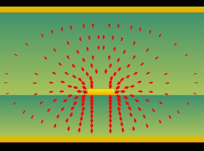
Illustration of field strength in multiple dielectric structure: As above, the area of influence can be reduced by bringing a ground plane closer to the trace. |