|
|
|
|
|
|
Determine H2 in Polar field solvers
Application Note AP8160
|
|
Determining H2 in Polar field solvers This note helps explain how H2 – or any height where copper is pressed into a prepreg – is defined in Polar field solvers, and helps you understand the question "Should the copper thickness T1 be added to H2 or not?" To understand the answer – read on...
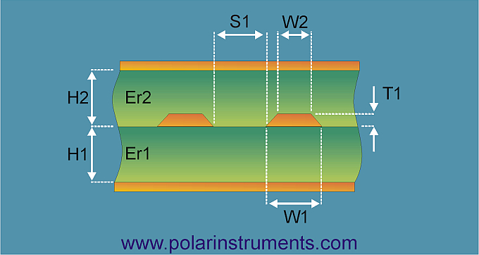
Fig. 1 Edge-coupled offset stripline structure Look carefully at the above edge-coupled offset stripline structure and you will see the copper traces are immersed or "embedded" in the surrounding H2 dielectric material. Where a Polar field solver structure shows the trace surrounded by a dielectric material like this we are showing the copper traces pressed into prepreg material. H1 shows core material – that is PCB substrate material that is fully cured with copper foils laminated to both sides – this material has a known height when pulled from stock, and will be specified on the laminate data sheet. The height shown by H2 cannot be calculated from a datasheet alone as the region is at fabrication time composed of prepreg which is part cured epoxy with glass fiber reinforcement (prepreg) – when heated and pressed this flows around the etched copper traces and the final H2 will be determined by the copper density of the traces on the layer and the flow characteristics of the resin when it is heated to start its final cure. |
|
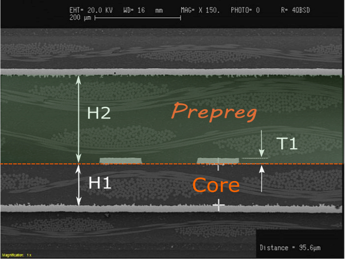
Fig. 2 Microsection of edge-coupled stripline
In Fig, 2 the stylised drawing of Fig. 1 is replaced by actual materials with, in this case, 2 sheets of prepreg. This is a precision microsection of a pressed and final cured PCB. H1 will, as described in the Fig1 text, be as the datasheet. H2 will be the finished pressed thickness once the resin has flowed into the available space between the copper traces. Think about this – the H2 will be greater when the copper density is higher and less when the Cu density is lower. There is another dimension left out for clarity – the isolation distance – which is H2 minus T1. It is easy to understand H2 when you work with a microsection as what you see is what you get. Predicting H2, though, requires some fabricator knowledge. |
|
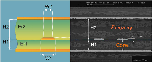
Fig 3 is a composite of Fig1 and 2 for clarity. The question posed at the start was how to calculate H2. From the above notes you will see "it depends..." Basically, it is the total thickness of the prepreg – less any press-out of resin at the edges of the panel – plus an amount depending on the copper thickness and density of the layer. A PCB fabricator can give you guidance on this base on their experience and manufacturing process. If you use a stackup design tool such as Speedstack PCB or Speedstack Si, there are built in pressing algorithms offering you a variety of methods for estimating the pressed thickness of the H2 or any prepreg based layer. These work with or without Cu density – but if you do have the Cu density per layer you will benefit from a more accurate simulation of the pressed thickness. From the field solver's perspective it always solves the dimensions that you – or Speedstack – determine. A microsection is always a valuable tool in proving that "you manufactured what you thought you manufactured." See how Speedstack calculates this dimension for you in AP507 Calculating dielectric height with Speedstack |