|
|
|
|
|
|
PCB designers guide to specifying controlled impedance (characteristic impedance) for fine lines
Application Note AP8517
|
|||
|
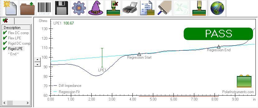
PCB designers guide to specifying controlled impedance (characteristic impedance) for fine lines PCB impedance control is a routine specification on many boards; as geometries shrink, fabricators making TDR impedance measurements will start to see the TDR trace rising over its length. Most of the reason for this is the DC resistance of the trace.* This DC resistance effect on the trace should not be confused with the characteristic impedance of the trace itself which is unchanging with length. Designers should ask their PCB fabricator to use a measurement technique which de-embeds (or removes) the DC resistance from the TDR measurement. A widely accepted technique – is LPE or Launch Point Extrapolation. This fits a line to the TDR trace and projects it back to the start of the test coupon – the launch point – where the probe and test coupon connect.
Launch Point Extrapolation So why not just test at the launch point? TDR testers used for impedance measurement look at the ratio of voltage reflected from the test trace in comparison with a calibrated 50 Ohm transmission line standard. At the launch point the reflection is masked by signal aberrations caused by the interconnect itself. For this reason test systems make the measurement further down the line over a stable section in order to minimise the errors introduced by aberrations at the launch. With lines of width 4 mil and above the DC resistance in the trace is so small that the trace remains flat. As traces get progressively narrower (and with thin copper) the trace will show more and more slope, introducing an error into the characteristic impedance measurement. LPE is a proven technique to remove this artefact. Why is the DC resistance ignored? Well, it should not be ignored, but it is a different specification from the characteristic impedance – and the two should not be lumped together. To think of this in another way – imagine a reel of coaxial cable of, say, 50Ohm or 75Ohm characteristic impedance with a DC resistance of one ohm per meter. Would you say the 50 Ohm cable was 60 Ohms if you used 10 meters? – No! the cable has a 50 Ohm characteristic impedance – and the resistance per meter is a separate specification. The same is true for PCB traces. Some PCB fabricators misunderstand this and lump the two specifications together then try to goal seek the Dk in a field solver to achieve correlation between measured and modeled values. This can lead to some very odd results – if the traces are very narrow solving for Dk without removing the DC resistance can lead to “that breaks the laws of physics!” kind of results where the “solved" Dk is less than that of the resin alone. So when PCB traces are narrow (approximately sub 60 microns or with very thin foils) fine it is imperative that a designer mandates that the PCB fabricator should use LPE or any other valid technique to remove the DC resistance artefact from the measurement before any goal seeking of Dk takes place. The Polar Track Resistance Calculator option for the Si8000m and Si9000e is useful for gauging how many ohms per unit length should be present. As a designer you need to ensure that your fabricator understands that they need to remove the DC resistance on fine line traces, so if you have a trace designed where the resistance is, say, 0.25 Ohms per inch or more, you should specify that the impedance should be measured on a TDR using the Launch Point Extrapolation method. *TDR traces may rise for two primary reasons: 1. There is DC resistance in the trace 2. The impedance is actually rising because the trace is tapering. To verify which is the case, simply test by launching from opposite ends, a varying impedance will rise from one end and fall from the other, a resistive trace will show a rising trace regardless of which end the measurement is taken. |
|||