
PCB Test Reduce programming and test times with the PFL Pin By Pin function
|
||
| Printer Friendly Version | |
|
Application Note 100
PCB Test Reduce programming and test times with the PFL Pin By Pin function |
| Printer Friendly Version | |
| Using the Pin by Pin function of
the PFL PCB fault locator can dramatically reduce the
programming and testing time for special or inaccessible
devices. Automated fault locators like the Polar PFL series which use pcb test and fault finding techniques such as Nodal Impedance Analysis and/or In-Circuit Testing rely for their speed on special probes and test clips that allow rapid scanning of whole devices or circuit modules. With the wide range of test clips and probes available most devices can be tested in just a few seconds. Using
the Pin by Pin option |
|
 The PFL edge connector display |
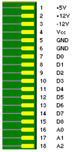
Using edge connectors On many boards signal and control lines are brought to the edge of the board via edge or RS232 D-type connectors. In a PC manufacturing environment, for example, ISA and PCI card connectors are readily available so PFL test fixtures designed to accept PC cards are widely used. The PFL inputs are hard wired to the card connector-simply testing each line of the card connector can often quickly verify large areas of a circuit board. If you use this method you'll need to make the decision whether to test each line as a separate component within your test program or to test the whole card as a single component. The default test parameters will be appropriate for most applications so circuit modules incorporating edge connectors can be tested at high speed. With up to 128 input channels available, in many cases virtually the whole card can be tested in a few seconds. Each connection on the edge connector can be assigned a descriptive pin name which will be displayed in the test list screen. |
| The service environment On boards mounted within an instrument, devices can be even more difficult to access. An installed board that is buried beneath a cable harness or located within an instrument card rack may be impossible to probe using the standard multi-pin probes. The device or module that could be tested with a standard test clip or probe with the pcb out of circuit may now only be accessible for testing via single pin probes. Separate tests or Pin by Pin? You can still test a pcb in this situation by writing a program in which each device pin is tested as a separate node-the board can then be tested with simple probes. This time-consuming process can be short circuited however by using the PFL Pin by Pin option. Using Pin by Pin the operator use a single pin test probe to test a multi-pin device or module as a device. The Pin by Pin option is part of the PFL Advanced Edit command. Select the device type then from the Edit menu select Advanced Edit; in the dialog box choose the ASA settings tab and click the Pin by Pin check box. Now when you acquire signatures for the device the Pin by Pin box is displayed with a prompt to probe the first pin. Probe the pin and press OK-the PFL780 will increment to the next pin number-repeat until the device is fully tested. Probing
special devices |
|
Polar Instruments Ltd polarinstruments.com Tel: +44 1481 253081 Fax: +44 1481 252476 © Polar Instruments 2002 |
 |
| © Polar Instruments 2002. Polar Instruments pursues a policy of continuous improvement. The specifications in this document may therefore be changed without notice. All trademarks recognised. | |