
PCB Test Understanding fault locator test methods can help reduce false FAIL results for good devices
|
||
| Printer Friendly Version | |
|
Application Note 103
PCB Test Understanding fault locator test methods can help reduce false FAIL results for good devices |
| Printer Friendly Version | |
| When using Nodal Impedance Analysis to test digital
devices on a pcb you will sometimes encounter difficulty achieving
stable signatures. Knowing how the Nodal Impedance Analysis fault locator
tests devices can help you develop techniques to reduce
spurious FAIL results for good devices. Nodal Impedance Analysis
signature stability |
|
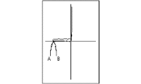 Unstable digital IC signature |
Observing the signatures using Live Instrument you may notice "jitter" on the screen as signatures jump between two or more shapes. This phenomenon will probably occur most often when testing digital ICs. It will produce effects similar to the signature in the diagram where the portion of the signature in the lower left quadrant switches rapidly between the shapes A and B. |
| Instability or oscillation in
signatures are often the result of capacitive circuits
and can be reduced by using the fault locator's facility
to insert a delay prior to each test - (the Pre Charge
function on the PFL series fault locators, the Step Rate
function on the T-series fault locators). Sometimes, however, a rapidly changing signature is the result of the combination of circuit configuration and the method the fault locator uses to produce the signature. |
|
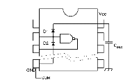 Typical IC input protection and decoupling |
Noise reduction decoupling Consider a typical digital IC under test as it appears to the fault locator. Note the decoupling capacitor on the Vcc pin of the IC. Many digital circuits utilise an even distribution of decoupling capacitors to assist in reducing noise, much of which is locally generated (e.g. by local lead inductance). Commercial circuits will typically employ one decoupling capacitor for each digital device. |
| Testing the device using
Nodal Impedance Analysis During IC testing the fault locator sequentially scans the pins of the IC and applies a sine wave stimulus between each pin under test and COM. Each pin will be stimulated by several sine wave cycles, the actual number will depend on the test frequency, the number of test ranges employed for the test and any delay specified. |
|
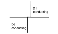 Idealised signature for input protected IC |
In the diagram to the left, as the
NAND input pin is tested the sine wave drive voltage
causes D1 and D2 to conduct on alternate half cycles to
produce the characteristic digital IC signature However, as D1 conducts during the positive half-cycle of the drive voltage it will allow charging current to flow in CDEC, the decoupling capacitor for the device. (Other decoupling capacitors on the supply line will appear in parallel with CDEC.) |
| The voltage on Vcc will therefore
rise as CDEC is charged. Under some combinations of test
voltage range and circuit configurations Vcc may rise
enough to turn on portions of the IC - the current drawn
will immediately discharge CDEC. This sequence of events
represents a rapidly changing impedance at the node under
test and causes the impedance signature to appear
unstable. You'll probably find the effect most pronounced
when a high current capacity range such as the LOW
voltage range is included in the test. Producing
stable signatures CAUTION: If you are using an Nodal Impedance Analysis/ICT fault locator such as the PFL series or TD8000 it is common practice to combine Nodal Impedance Analysis and ICT into a single test. Because of the way the fault locator switches between Nodal Impedance Analysis and ICT it is essential that you use both COM lines, i.e. connect the board GND to the left COM socket and Vcc to the right COM socket. |
|
Polar Instruments Ltd polarinstruments.com Tel: +44 1481 253081 Fax: +44 1481 252476 © Polar Instruments 2002 |
 |
| © Polar Instruments 2002. Polar Instruments pursues a policy of continuous improvement. The specifications in this document may therefore be changed without notice. All trademarks recognised. | |