| PCB fabrication considerations for lossy transmission lines | |||
Polar products for use with lossy transmission lines
Why do I need to know about PCB transmission line losses?
You may have heard discussions about loss testing, or modelling of PCB losses and if you haven't yet, it is most likely that you will be hearing or seeing requests regarding PCB losses in the coming months. For a PCB fabricator the considerations necessary for building repeatable lossy transmission lines are different from those necessary for lossless (impedance controlled) lines. This note seeks to paint a picture for you to begin to understand the questions your design customers may be asking you.
What is behind this? – first, impedance control and now, lossy transmission lines
First, to set the record straight: a transmission line is always a transmission line in the context of a PCB a uniform trace (or traces) running over, or sandwiched between, dielectric materials. Whilst signals were running from 100MHz up to a couple of GHz we could "assume" the transmission line on the average PCB was lossless. Now, new generations of silicon are appearing which allow designers to run multi-GHz signals on FR4 at these frequencies losses are significant. However good the silicon is, the PCB still needs to work within expected limits, so modelling and measurement of loss will become increasingly important.
How will this effect me as a fabricator?
Thinking back again to impedance controlled PCB traces, fabricators needed to understand the line widths and layer separations required to produce the required impedance. Larger dielectric separations raised the impedance and making traces wider reduced impedance. With these two adjustments the control of impedance on traces is a relatively straight forward operation. So for lossless operation the PCB fabricator could choose from the following to control the impedance:
Lossless lines:
|
Line width |
first order effect |
|
Dielectric constant |
second order effect |
|
Trace length |
no effect** (design consideration) |
|
Copper roughness |
no measurable effect. |
Transmission lines
operating at lossy frequencies:
|
Trace length |
first order effect (design consideration) |
Loss tangent |
first order effect |
|
Dielectric separation |
second order effect |
Trace profile |
2nd or 3rd order effect |
|
Dielectric constant |
no effect |
Now read the above lists again see how the factors
that determine loss are quite different from those that
determine lossless impedance.
When designing multi-GHz lines on FR4 or derivatives
designers will need to be cautious about line length,
and as a fabricator you will need to take care with base
material specification with special regard to loss
tangent.
Loss testing methods
Testing is still the subject of much debate. You may receive questions about some of the better known test methods, RIE test,
SET2DIL test, SPP test,
S-parameter test or VNA test. A variety of techniques may be used
for measuring losses, each with its own strengths and weaknesses; over time some of these will become more prominent, and others will fade away. RIE is one method that showed promise, but has now been displaced as it proved difficult to correlate results between measurement sites. SET2DIL is an increasingly popular proposed method; however, all the methods are jostling for adoption; it is likely that the industry will settle on just one or two methods as loss testing becomes mainstream in the next few years.
Polar's Atlas PCB lossy line test system supports SET2DIL (Single-ended TDR to Differential Insertion Loss); this SET2DIL paper describes the method.
A
professionally documented layer stackup.
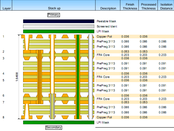
Figure 1 Speedstack Si documented stackup with material types and thicknesses specified
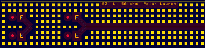
Figure 2 Lossy line test coupon (sample coupon for illustration purposes only)
What possibilities will this create for me as a fabricator?
Learning the "language" of lossy transmission lines will help you when your customers start to specify requirements for designs which employ very high speed transmission and silicon families designed to work with lossy transmission lines. Familiarizing yourself with the material properties that effect losses will help you understand your customers' requirements. If you already make controlled impedance boards you may use a CITS25 / Si6000 or Si8000m controlled impedance field solver. For lossy line calculations Polar's Si9000e allows you to model transmission line losses up to typically 140GHz.
Stackups/coupons
Speedstack is a layer stackup design package that lets you document and manage the layer stackup, something which will become more important as losses become part of the customer specification (Speedstack and Si9000e are available as a bundle Speedstack Si.) Si9000e allows you to run a whole range of "what if" scenarios for a range of materials before you take a board to the prototype stage. Finally, in preparation for future testing requirements, CGen Si coupon generator supports attenuation test coupons.