|
|
|
|
|
|
Laminates, losses and the Si9000e – choosing a PCB laminate
Application Note AP8173
|
||||||||||||
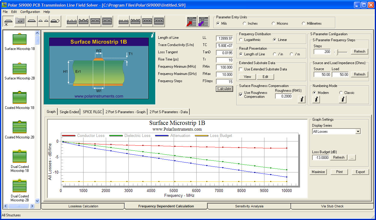
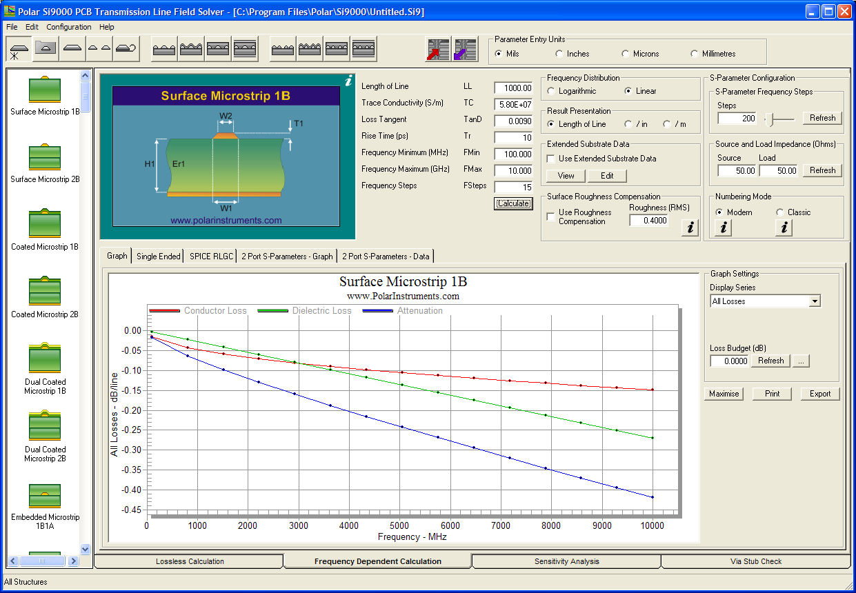
Selecting the most appropriate PCB materials for your ultra high speed digital applications Do you remember a time when PCB material selection was simple? For run of the mill applications choose "vanilla" flavored FR4 and for high speed applications, perhaps either a ceramic loaded core or PTFE based substrate. Whilst these two options still exist at the extremes of the market the last few years have witnessed a stream of new "mid market" core and prepreg materials which temptingly offer increased high speed performance and more standard processing methods than more exotic materials. There is a place for all the above materials in the market but both the EE putting together the "platform specification" for the new design and the PCB fabricator responsible for its realisation are faced with a bewildering array of materials with a mix of choices from ease of processing through to reliability requirements and onwards to signal integrity capability. This application note deals with the signal integrity angle and how to use the Si9000e to make the best choices for material selection when trading cost versus signal integrity performance. From an ultra high speed digital perspective – what characteristics most affect signal integrity? High speed serial communications on PCBs increasingly operate at a speed where signal loss is the predominant characteristic impacting on signal integrity and chipsets will have an acceptable "loss budget" which must not be exceeded if the circuit is to perform at maximum data rates. There are three primary drivers for losses: 1. Line length (only applicable at the design stage) 2. Dielectric loss (by appropriate material selection) 3a. Copper loss – (cross section area – stackup design) 3b. Copper loss due to surface roughness (by material selection – and / or stackup) You can use the Si9000e lossy line field solver to get a very rapid "feel" for which of the above drivers is having most effect on your particular design. Modelling line length Taking line length first – simply enter your chosen transmission line structure, along with the material characteristics from the laminate supplier datasheets. Enter the frequency band of interest and experiment with how long your transmission line can be before loss budgets are exceeded; in the example below we see that a line length of 14 inches meets the loss budget of –13dB and a 17 inch line exceeds it. Click on the graphics or links below to see the Si9000 results for the line.
Figure 1 Modelling dielectric loss Second, by looking at dielectric loss you can either enter a single loss tangent per material and run the Si9000 multiple times over your frequency range of interest to see the effect of loss tangent on your budget. You can also enter tables of Er and Tan Delta for a range of frequencies if they are available to you. (Note for advanced users: from 2009 versions onward the Si9000e will interpolate the data to ensure that any extracted frequency characteristics are causal.) The examples below (Figure 2) compare a one inch trace on standard FR-4 with its typical value of tan delta of 0.022 with a higher performance material, tan delta 0.009. Click on the associated graphic below to see the Si9000 results for each material.
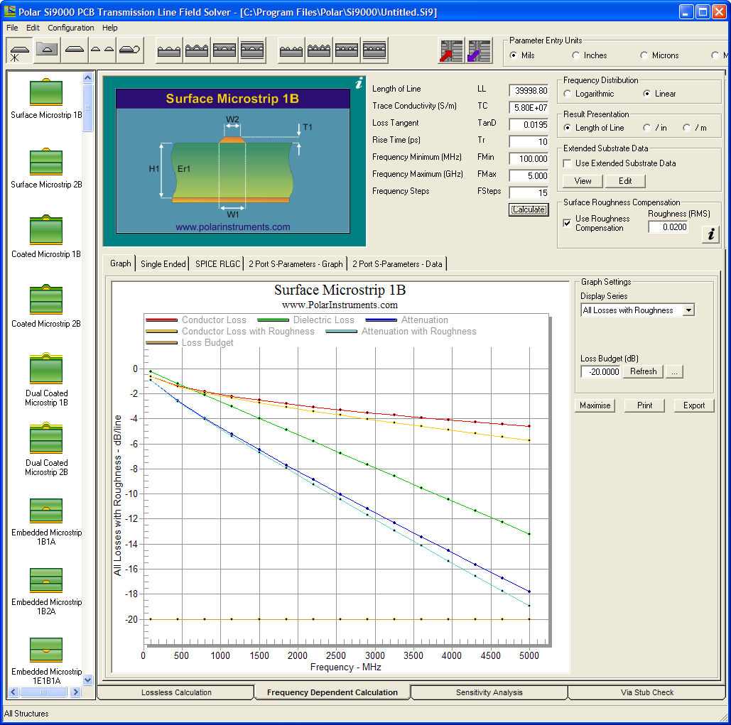
Figure 2 Two methods need to be used when looking at copper losses (conductor loss) due to cross sectional area. First, you can extract the conductor losses and ignore the effects of roughness. Microwave designers used to minimise these losses by achieving their required impedance with wide traces and large dielectric separations. However in digital designs device physical dimensions usually limit your freedom on line widths. Modelling surface roughness Finally, you can add in the modelling which calculates the losses due to the RMS roughness (in this case a physical dimension — not a voltage!) i.e. the RMS of the peak to trough height variation on the copper surface. It could be that by using a smoother copper you can save money with a lower performing dielectric material. However, you need to model each case to find which of the above is the main influencer in your design. Click on the graphics below to show how a typical range of values for RMS roughness (0.6 µm (0.02mils) for stripline, 1.6µm (0.06mils) for surface microstrip) can prove the difference between meeting or exceeding the loss budget for 40 inch total trace length.
Figure 3 Commercial approach from the product design specifier or the fabricator From the design authority's perspective it may seem best to "lock down" to a very tight material spec possibly even specifying the brand and type of material to be used. This approach does have its place but it is also valuable to consider allowing the fabricator more freedom to choose materials and take a more generic approach by specifying the material choice according to IPC slash sheets. From the fabricator's perspective a tightly specified material requirement makes the specification very easy to interpret but leaves no freedom to work on the best cost / material trade off. Another benefit of a more generic specification of materials gives the ability to substitute an equivalent in times of material shortage or lengthening lead times. The above choices can be down to company policy or the regulatory environment of the end use product- however, it is always worth keeping an open discussion channel between the three parties of laminate supplier, PCB field applications engineer and the original design specifier. What if you don't use modelling tools to explore your design space? Chances are that you will either pay more than is necessary to produce a product, or even worse, discover that the design struggles to meet its high speed performance specifications. Using the Si9000e will help you: Hold discussions between fabricator and supplier that result in the most cost effective material choice and stackup design for your chosen application and allow where possible rapid material substitution in the event of material price rises or shortage of supply. |