|
|
|
|
|
|
Via Pad / Anti-Pad Impedance Calculation
Application Note AP8178
|
|
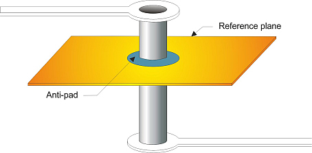
Note: This note describes single ended vias. Si8000m and Si9000e now also support models for differential vias – see the associated Application Note, Si9000 Via Checks The Si9000 provides for modelling plated through hole (PTH) vias with respect to impedance and signal integrity in order to allow the designer to ensure a constant impedance is presented to a signal as it propagates between devices. The Si9000 Via Checks tab includes via stub checking (see Polar Application Note AP8166) and via pad/anti-pad calculation. The anti-pad is the void area (shown as the blue annular ring in the diagram below) between the pad and the copper of the plane. It should be designed so that it maintains the impedance of a transmission line as it passes through the plane.
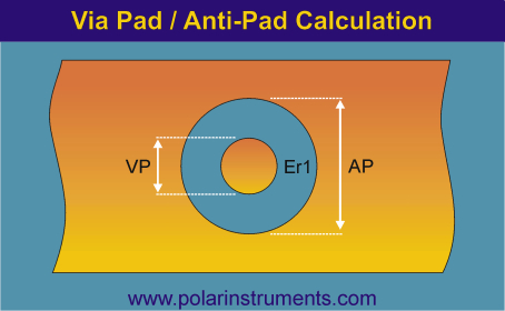
This impedance value will of course only apply to the 2D cross section, where the via passes through the reference plane. It will, however, remove another section where a signal reflection may occur. The Si9000 Via Pad/Anti-Pad Calculation will determine the effect of the via pad size in relation to the anti-pad size as it passes through a reference plane. Via pad / anti-pad impedance calculation The following worked example demonstrates the Via Pad / Anti-Pad Calculation included in the Si9000.
This example assumes a transmission line characteristic impedance of 50 Ohms; choose a via pad size (VP) of 12 mils (0.3mm) and calculate the anti-pad (AP) size that is required to present a nominal 50 Ohm impedance at this point. For this calculation it is also necessary to specify the dielectric constant (Er1 illustrated above) in the region of the via. A material such as FR-4, which is a composite of resin (Er 3.2) and glass fibres (Er 6.1), will have a bulk Er of around 4.1 with significant local variations. It is reasonable to assume that the Er value in the immediate vicinity of the via will be lower than the bulk Er of the dielectric material as more resin will tend to flow into this type of region. For more information on the effects of resin rich areas on impedance please read Polar Application Note AP165. With this in mind, for a standard FR4 material with a bulk Er of 4.1, Er1 in this example has been specified as 3.5. Add the values of the via pad diameter, VP, of 12mil (0.3mm) and the Er1 of 3.5 to their respective fields. Move the slider bar for the anti-pad diameter, AP, until the Impedance (Zo) field displays 50 Ohms (alternatively, type the value into the Anti-Pad Diameter text box.)
It can be seen from the example above that to achieve the 50 Ohm target impedance the anti-pad is quite large when compared to the via pad. The anti-pad size could be reduced by, for example, removing the non-functional pads from the reference planes. For this example assume the drilled size via pad diameter, VP, is 8mil (0.2mm). This will in turn reduce the anti-pad diameter, the AP dimension, to 38mil (0.95mm). Note: for this calculation the drilled size is required, not the finished size.
Note that as signal speeds increase it becomes more important to take via stub lengths and impedance into account. For detailed analysis you may wish to employ a 3-D solver. However, in many cases this straightforward check will ensure that any major mismatches are removed before you resort to more detailed analysis. Polar Instruments will be happy to discuss issues relating impedance and signal integrity issues with customers with Polarcare contracts. Please contact Polarcare with your Polarcare number at polarcare@polarinstruments.com. |