|
|
|
|
|
|
How PCB stackup properties impact crosstalk
Application Note AP8210
|
|
|
The PCB stackup in a high-speed digital design is responsible for creating or preventing some of the most common signal integrity problems. The PCB stackup defines impedance and suppression of radiated emissions. Another area of PCB stackup engineering that is not often considered is crosstalk, something which may not be examined until the PCB routing phase. In many cases, crosstalk is never considered and is only identified when there is a problem with a prototype of the design. While it is possible to set routing constraints that will keep crosstalk undetectably low, not all designs have this luxury. Simple digital designs with low net count can certainly plan routing channels and set minimum spacing constraints that keep crosstalk undetectably low. When I/O counts become large and trace density increases, crosstalk becomes something to be examined at the beginning of the design cycle. Some simple principles regarding dielectric thickness and material selection can help designers control crosstalk. How PCB designers typically control crosstalkMost PCB designers try to control crosstalk without performing an estimation of the expected amount of crosstalk for a given edge rate. For some designs, this is acceptable as the trace density and edge rate are low enough that crosstalk is also expected to be low. Some digital designs still use slower serial buses and have slower GPIOs, which also reduces expected crosstalk. However, most modern designs do require some basic approach to suppressing crosstalk, which often includes:
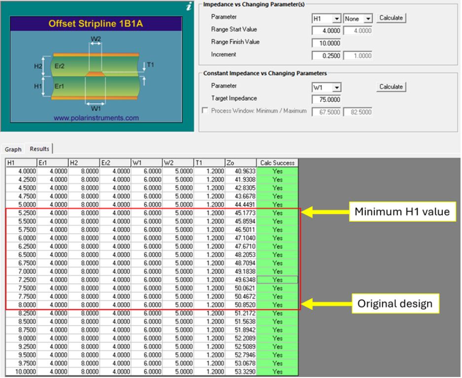
The use of guard traces is particularly problematic as it works in some situations but fails in others. There is also the matter of differential crosstalk, which is related to the inter-pair spacing as well as pair-to-pair spacing. For example, see the excellent article by Bogatin and Simonovich in Signal Integrity Journal. There's one thing that SI experts and EMC experts can agree on: the PCB stackup is the place to start implementing measures to control crosstalk and EMI. Many of the common problems in these areas can be suppressed by understanding how stackup properties impact crosstalk. For now, we can look at two areas: impact of dielectric constant and distance to the nearest ground plane. How distance to ground impacts crosstalkFirst, let's examine a common approach of moving ground closer to a victim trace by decreasing the dielectric thickness in a layer. The correct design approach to reduce crosstalk in both single-ended and differential interconnects depends on whether those interconnects require impedance control. For single-ended interconnects that do not have an impedance requirement, it is a simple matter to move ground closer to a trace if the trace in question is a victim of excessive crosstalk. Doing so reduces trace self-inductance and increases its self-capacitance; mutual inductance and mutual capacitance will also both decrease, leading to lower inductive and capacitive crosstalk. The net result is lower forward and backward crosstalk. When the victim interconnect has an impedance specification, the allowed reduction in dielectric thickness is quite small and can be calculated easily using sensitivity analysis. The image below shows sensitivity analysis results for a 50 Ohm single-ended symmetric stripline (1 oz./sq. ft. copper weight) with trace width of 6 mil in a material with Dk = 4. The sensitivity analysis results show that one of the ground planes can only be moved by approximately 2.75 mil while keeping the trace width the same before the trace impedance falls outside the typical tolerance value of +/-10%.
What is the effect on crosstalk in this situation? If we have two of these traces with an edge-to-edge clearance equal to W, then the crosstalk coefficient in each situation is:
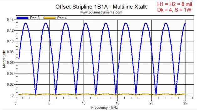
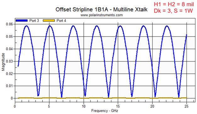
If instead, we simply increased the spacing between the traces to 1.5W, the crosstalk coefficient in each situation is: These results should illustrate that the more effective approach is to increase the spacing when impedance control is required, assuming you do not want to change the trace width. Maintaining impedance control while moving a ground plane Suppose that we move a ground plane to control crosstalk, but we also adjust the trace width so that the trace still has the same impedance, and we maintain the position of two of these traces. In the above situation, if we were to take the stripline and reduce the distance to one of the ground planes by half, the required trace width, new spacing, and crosstalk coefficient would be: What if we still wanted to maintain the same 1W spacing value as in the original situation with our 6 mil symmetric striplines separated with an edge-to-edge clearance of 6 mil? By maintaining a 1W spacing value, the new edge-to-edge clearance is X mil. The crosstalk coefficients in the original and new situations are: As we can see, bringing ground closer to the traces but maintaining the same edge-to-edge spacing ratio of 1W does not reduce crosstalk — it actually increases crosstalk compared to the original 6 mil width/spacing striplines with H1 = H2 = 8 mil. This shows that the spacing ratio will need to be increased when attempting to decrease crosstalk at a constant spacing:width ratio by moving the ground plane. Influence of the dielectric constant with impedance control The other lever we can pull in these situations to reduce crosstalk is to switch the dielectric material to one with a smaller dielectric constant. The dielectric constant determines the self-capacitance of a transmission line and the mutual capacitance between two transmission lines. If an existing trace design is modified by changing the dielectric constant, the dielectric thickness or trace width will need to change to compensate and keep the trace impedance constant. Consider the original stripline design with 50 Ohm impedance at 6 mil width on a Dk = 4 substrate material (H1 = H2 = 8 mil). If the dielectric were changed to a material with Dk = 3, we can examine the new backward crosstalk coefficient: In both cases where we maintain impedance control, the crosstalk is lower than in the original backward crosstalk coefficient with 1W spacing (Kb = 0.0476). This illustrates one of the major reasons to use lower dielectric constant in a high-speed PCB, and yet it is the reason that most so-called experts never discuss! To capture the full influence of dielectric constant, transmission line geometry, a frequency domain analysis is needed and is normally specified in interface standards. For the example shown here, we can also see the crosstalk reduction in the frequency domain by comparing the multi-port S-parameters for the original striplines separated by 1W and the same stackup with smaller dielectric constant (H1 = H2 = 8 mil, Dk = 3). The multi-port S-parameter results below show a reduction in the peak NEXT value of 56%.
Multi-line crosstalk results for the original stripline design: trace width = 9.11 mil and Dk = 4 dielectric material
Multi-line crosstalk results for the modified stripline design: trace width = 9.11 mil and Dk = 3 dielectric material With an easy-to-use 2D cross-sectional field solver that is specialized for PCBs, designers can take the guesswork out of crosstalk calculations. To take the risk out of your high-speed PCB design, use the Polar Instruments Si9000 Insertion Loss Field Solver Contact Polar to learn more. |
|