|
|
|
|
|
|
PCB Stackup or Buildup – a brief history
Application Note AP537
|
|
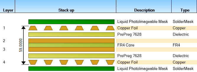
PCB Stackup or Buildup – a brief history Stackup, or buildup of PCBs, has grown in importance over the last decade. From the early days, when PCBs functioned primarily as interconnect, the need for stackup was minimal – on a single sided PCB the stack is a “stack” of one piece of clad material. Even the board thickness was rarely a consideration unless it needed to plug into an edge connector. However, with the advent of multi-layer PCBs the stack of materials starts to become more critical – and, as always, cost is often the underlying driver. Stackups can range from the simplest 4-layer PCB to complex stackups requiring sequential lamination. Let's take the humble 4-layer PCB – designers not familiar with PCB fabrication may be forgiven for thinking the 4-layer board is usually comprised of two double-sided rigid PCBs bonded together with another layer of unclad material. It may come as a surprise that most 4-layer boards are stacked – not as described, but as a central 2- layer PCB with two sheets of copper foil laminated on the outside with the bonding provided by a layer or two of glass cloth “pre impregnated” with uncured resin (prepreg).
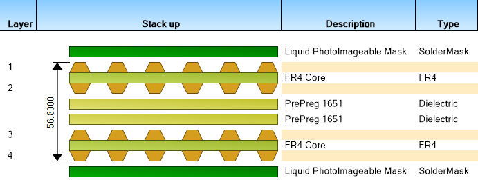
4-layer foil build stackup Foil and core builds This most basic (and simplest to build for the fabricator) 4-layer stackup is called a “foil build” (shown above) and a foil on the outer layer of the stack is the most common build for even higher layer count boards. You may be asking, "When would you laminate two 2-layer boards together?" Most often in microwave applications where expensive microwave materials are laminated together with a lower cost internal bonding layer. This type of 4 (or greater) layer stackup (shown below) is called a “core build” as it comprises core materials on the outer layers.
4-layer core build stackup
Outside of the microwave world – designers called to work with ever higher device integration need more layers for routing – some of those layers or layer groups (sometimes called cells of layers) may comprise higher speed materials. These may require different processing – but invariably the high speed materials are higher cost so for volume use designers will try to build stackups with a mix of appropriate materials for the layer type – so leading to more complex stackups.
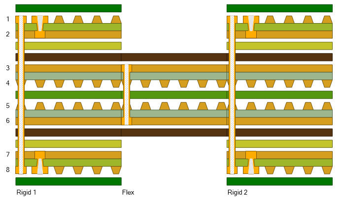
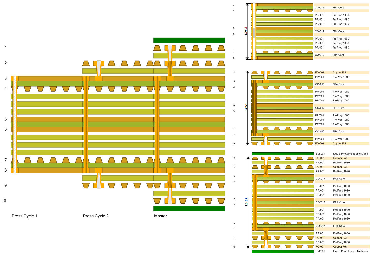
Flex-rigid stackup Sequential lamination By taking the PCB multiple times through the production process boards can be built with drilled holes that only appear to go through parts of the stack – the process for this type of complex stackup is called sequential lamination. It can have benefits for both signal integrity (shorter vias) and give more flexibility in interlayer interconnect than a traditional stackup, which uses holes drilled through the entire board. HDI builds The icing on the cake for complex rigid multilayers is the HDI build – where additional layers are laminated with multiple passes through the production process and laser drilled to give even more interconnect density and enhanced signal integrity. A typical HDI build with its three press cycles is shown below. From the stackup perspective, consideration needs to be given to glass styles that benefit laser drilling such as flat or spread glass.
Multiple press cycle HDI build Complex? Yes – and from humble origins the PCB has developed into a complex interconnect device containing basic components included fabricated inductors, capacitors and transmission lines. The OEM PCB technologist has the task of ensuring that the layer stack is designed in a cost effective and reliable way that is both appropriate for the application and the lowest cost and easiest to fabricate. Flex rigid PCBs bring in a whole new layer (excuse the pun...) of complexity which will be covered in another note. |