|
|
|
|
|
|
Choosing reference planes for controlled impedance structures
Application Note AP539
|
|
Working with controlled impedance structures in Speedstack Polar customers sometimes ask "Can I reference a transmission line to a non adjacent plane?" This need can arise when lines must be made a sensible width when working on thin layers. It is usually performed by opening an aperture in the adjacent plane above or below the line and then referencing to the appropriate plane(s). Speedstack achieves this when you add or modify a structure; for example, when adding a structure the "Advanced" button allows you to reference through mixed planes to non adjacent layers. Some users refer to the bounds of the structure as the impedance cell. The cell is graphically represented in Speedstack as shown below – the sequence of pictures illustrates
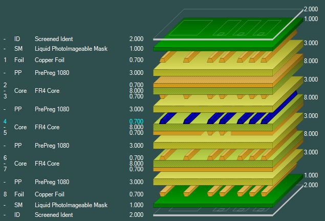
Using Speedstack's editor to choose reference planes For the example stack below, add a controlled impedance structure to signal layer 4 (highlighted in the stackup below.)
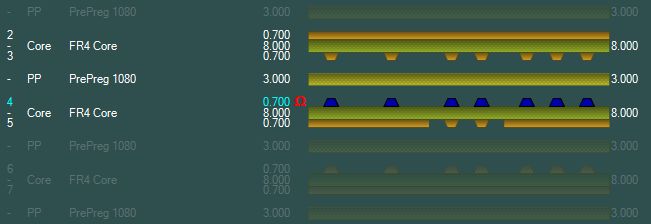
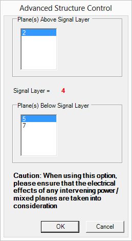
Note that in this stackup layer 5 is a mixed signal/plane layer; potential reference planes for signal layer 4 are therefore plane layer 2, mixed signal/plane layer 5 and plane layer 7. Using Speedstack's Advanced Structure Control, signal layer 4 is first referenced to plane layers 2 and 5
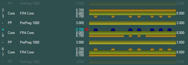
Advanced Structure Control is then used to reference signal layer 4 through mixed layer 5 to layers 2 and 7
Adding a structure Click Layer 4 to select it, ensure it is highlighted (in blue, above) then click the Controlled Impedance tab. The Add Structure button is displayed.
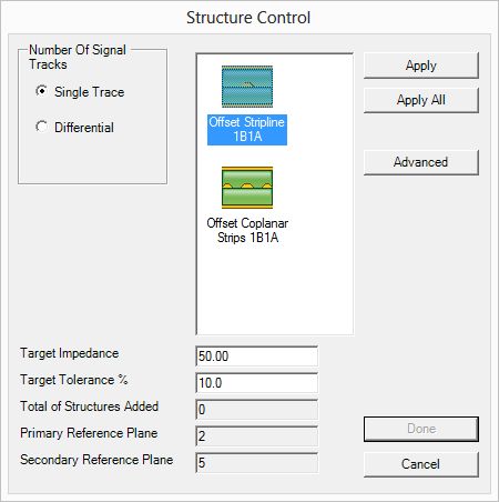
Click the Add Structure button; the Structure Control dialog is displayed containing the controlled impedance structures applicable to the selected layer in the stack.
Choose values for the target impedance and tolerance. If necessary, resize the Structure Control dialog to view all structures. Click the Single Trace, Differential or Broadside option button as appropriate (in this example, choose Single Trace | Offset Stripline 1B1A with a 50 Ohm impedance.) Note: Broadside only appears as an option where the signal trace is between two reference planes and Differential is selected. Specify the values for Target Impedance and Tolerance. Choosing reference planes As there are multiple reference planes available (layers 2, 5 and 7) it will be necessary to specify which planes to use for this structure. Click Advanced to display the Advanced Structure Control dialog.
Choose a reference plane from the list of available planes. In the example structure plane layer 2, mixed plane 5 and plane layer 7 are available for reference. In this example choose mixed signal/plane layer 5. Press OK to confirm. The chosen reference planes are shown below.
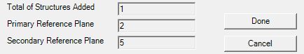
Repeat for all structures to be added. Click Apply for each structure then click Done to finish. In this example, choose a single structure. Layers with controlled impedance structures are indicated by a red Ohms symbol.
The stackup window changes to reflect the selected signal layer and its associated reference planes, in this case, layers 2 and 5. The applied structure is displayed in the Controlled Impedance pane.
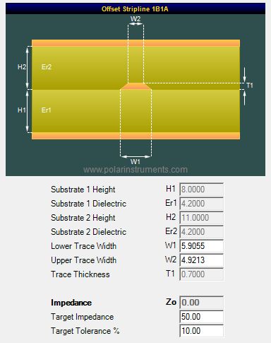
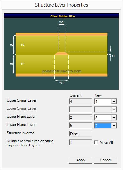
The structure window displays the parameters of the controlled impedance structure. Fields shown "greyed out" are values derived from the choice of materials in the stackup. Changing the reference plane To reassign the reference plane from layer 5 to layer 7 click the Structure Layer Properties button
The Structure Layer Properties dialog is displayed
Reassign the layers from the Current settings to the New and click Apply – the editor displays the redefined structure with reference planes on layer 2 and layer 7. Note: if plane layer 7 is chosen as reference, it will be necessary to take into account the electrical effects of mixed signal/layer plane 5.
For the structure, enter appropriate values for lower and upper trace widths. Click the Calculate Displayed Structure button to display the impedance value of the structure with the current parameters. The parameters may then be varied to alter the value of the final impedance. In the example above, the trace width can be fine-tuned in order to approach the value of the target impedance; other parameters are changed by modifying the stackup dimensions (for example, core thickness H1.) Hint: clicking Apply All in the Structure Control dialog adds a single instance of all structures matching the stackup layer and the chosen criteria; you can then choose the structure producing the value nearest the target impedance and delete the structures that are not needed. Speedstack offers significant advantages over the "structure at a time" approach of a stand alone impedance field solver. By attaching all the impedance structures to the stackup, the task of managing materials and repeat designs with the same or similar stackups and providing the appropriate professional documentation is achieved in a fraction of the time when compared with modifying structures one at a time. To see Speedstack for yourself – simply email polarcare@polarinstruments.com or call your local Polar office. |