|
|
|
|
|
|
What is insertion loss?
Application Note AP8196
|
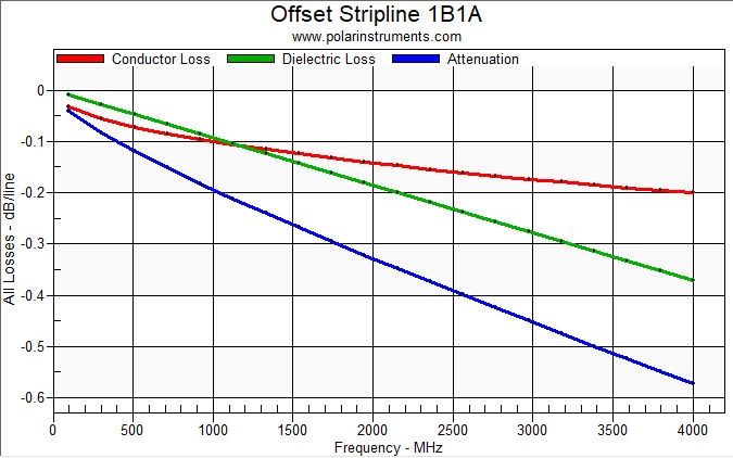
Insertion loss Application note AP120 What is controlled impedance? discusses the importance of considering traces on high speed PCBs as transmission lines of known – and controlled – characteristic impedance. This application note is an introduction to the cause and effect of insertion loss which becomes predominant as you push upwards from 3GHz. Typically, impedance control will be necessary on PCBs running in the 100MHz to 3GHz frequency range, where signal integrity will be significantly affected by signal reflections. Above these frequencies signal loss will be an increasing (and ultimately predominant) factor in signal integrity. Energy is lost from a signal as heat in the conductor (i.e. the PCB trace and ground planes) resistance (it's a function of the material and plating used) and as heat in the dielectric caused by the inherent material properties of the base material iteslf. Total loss is therefore the sum of conductor loss and dielectric loss. The dielectric loss mechanism is similar to that in a microwave oven; heat is generated in the food (where it is desirable) and in a PCB dielectric – where such loss is undesired or at least needs to be understood and managed. At low frequencies, conductor loss exceeds dielectric loss; dielectric loss, however,increases at a higher rate than conductor loss and will overtake it as a proportion of total loss (at around 1.1GHz in the chart below.)
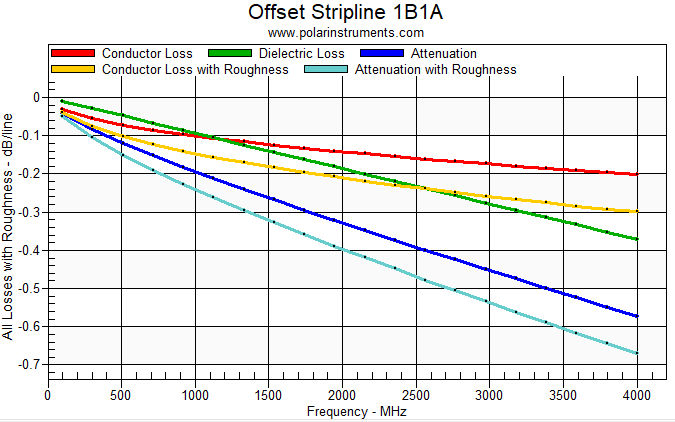
Conductor loss and dielectric loss Surface roughness In order to provide good adhesion between copper and dielectric materials in core layers, PCB materials vendors control the roughness of the associated copper layers (typically by chemical treatment). Since the roughness is a random quantity it is commonly specified in terms of the rms (root mean square) height, h, of the surface unevenness. The surface roughness of the copper layers will have no effect on current at low frequencies as, at low frequencies, the depth of current penetration will exceed the value of h. Chemistry suppliers and foil manufactures are researching ways of making the copper smoother whilst still achieving sufficient adhesion to ensure the desired reliability. At high frequencies, however, (i.e. in the GHz region), the skin effect (see AP8155) will be significant as most current now flows in the outside of the conductor (in a very narrow skin on the conductor – hence the name.) This will introduce signal attenuation at high frequencies, increasing conductor loss (shown in yellow below) and therefore total loss (shown in light blue below.)
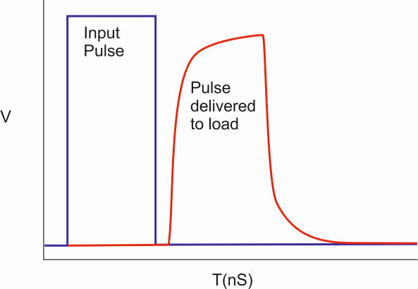
Loss including surface roughness Why do we need to worry about insertion loss? At high frequencies signal loss produces signal attenuation and distortion; the signal will be attentuated by conductor resistance and leakage in the laminate material; a signal pulse will be distorted as loss unequally affects each of the signal harmonics. Loss is frequency dependent so each successive harmonic will be increasingly attenuated; the resulting amplitude and changes means the signal at the load will be a distortion of the original – its front edge is rounded and its amplituded reduced as shown below.
Insertion loss on PCBS The behaviour of the ideal transmission line is independent of frequency. Transmission lines are used to deliver high speed signals with minimum degradation. In the real world, however, minor differences show up as the operating frequency changes. The primary physical characteristic that causes PCB transmission lines to deviate from the ideal is the dielectric constant, Er, of the base material. The design of high-speed circuits therefore requires a knowledge of the dielectric constant and loss parameter, Tan d, of the substrate. This is particularly important when using FR-4 material because variations may be encountered among different vendors and even between different orders from the same vendor. Testing for insertion loss on PCBS It is not uncommon for PCB traces to be inaccessible for testing. In addition, traces may be too short for accurate measurement and may well include branches and vias which would also make exact measurements difficult. Adding extra pads and vias for test purposes would affect performance and occupy board space. PCB testing is therefore normally performed, not on the PCB itself, but on test coupons integrated into the PCB panel. The coupon is of the same layer and trace construction as the main PCB and includes traces with precisely the same characteristics as those on the PCB, so testing the coupon affords a high degree of confidence that losses measured on the coupon reflect those on the board. Polar Atlas software employs multiple test methods to extract frequency dependent loss characteristics when used in conjunction with suitably designed test coupons and Atlas precision GHz probe assemblies. Test methods include Delta-L, SET2DIL (Single-Ended TDR to Differential Insertion Loss) for extraction of differential insertion loss and effective Er from a single-ended test and a suitably designed coupon, SPP (Short-Pulse Propagation) methods as called for in IPC-TM-650. Insertion loss may also be measured using a Vector Network Analyser (VNA); interconnect of the coupon is a more challenging task than for impedance measurements and the design of the coupon more complex and the cost of the probing solutions inherently higher than those for impedance test. Modelling insertion loss Many tools are available to model insertion loss, including the Polar Si9000e which models insertion loss using Boundary Element Method (BEM). The Si9000e is able to split out and predict both dielectric and copper losses and further simulate the impact of surface roughness on insertion loss with a variety of popular methods (Hammerstadt, Groisse and Huray). |