|
Modeling controlled impedance structures with a planar resin layer
PCB stackups do not encapsulate the signal traces in homogenous material and depending on the stackup design the signal trace may sit in a significant resin rich area. There are a number of ways of treating this from a modelling perspective.
Before going into detail on the best model for your application – it is worth noting that as traces become thinner the Zo vs distance trace on your impedance measurement system may exhibit a in increase in apparent Zo as the signal propagates the trace. This is not noticeable on broader traces. This apparent rise is an artefact of the trace resistance – and should be removed from the measurement either directly by using Launch Point Extrapolation (LPE – see AP8517) or DC resistance compensation in a CITS – or by inspecting the TDR trace from other systems to ensure you manually remove the offset) before any correlation is attempted.
This is especially the case if you are considering “goal seeking” to find the apparent Dk. Dk has a second order effect on Zo, and if you do not remove the DC resistance artefacts first you will settle on an erroneously low value for Dk.
Si8000m / Si9000e resin layer models
In Si8000m and Si9000e there are a range of off the shelf structures to allow you to model each scenario. Download the Si8000m / Si9000e structures Resin_layer_models_typ_fr4.sip and Resin_layer_models_hi_perf_laminate.sip that illustrate the concepts discussed in this note.
Having removed any DC resistance offset from the trace (either with DC resistance compensation or Launch Point Extrapolation) you can then choose the best structure for your application. For routine non demanding applications the "standard" structures below will be “good enough” in most cases.
How do I model a planar layer of resin adjacent to the signal trace?
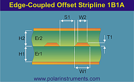
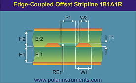
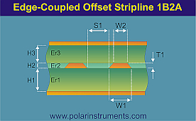
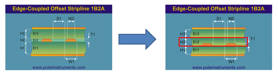
The Si8000m / Si9000e Edge-coupled Offset Stripline 1B2A (one dielectric below and two above the trace pair) can be accurately modeled as shown in the illustration on the left image below; the actual structure needed is 1B2A structure shown on the right. H2 may be set to the copper thickness plus a small additional thickness to model the buttercoat of resin (the red region shown in the structure below right.)
Si8000m and Si9000e offer a range of structures to best suit your application.
The Si8000m / Si9000e offer a range of structures – which you choose depends on how critical your tolerance requirements are and the type of base material you are using. Remember that Zo varies inversely with the square root Er and so Er has only a second order effect on impedance compared with trace width.
|