|
|
|
|
|
|
Create and professionally document PCB stackups in an instant
|
||
|
|
||
|
Speedstack PCB – using Si projects to fine tune PCB stackups Can't view the video? Click here |
||
|
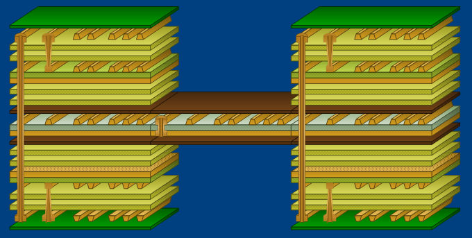
Speedstack PCB – PCB stackup / Impedance field solver package Speedstack PCB stackup design tool is a packaged combination of the Si8000m field solving impedance calculator and the Speedstack professional layer PCB stackup design system. If you need both impedance calculation and layer stackup/build up documentation the Speedstack PCB offers a considerable saving over purchasing separate licenses. For PCB fabricators, Speedstack PCB interfaces with the industry standard Polar Si8000m PCB Controlled Impedance Field Solver. It includes a link and license for Polar’s Si8000m, using the proven Polar Si8000m multiple dielectric boundary element field solver to provide the impedance data for the stack. Ideal for both rigid and flex-rigid stackups Speedstack PCB allows OEM designers to create accurate and efficient rigid and flex-rigid PCB stackups in just a few minutes, with error-free documentation for tighter control over the finished board. For PCB fabricators, Speedstack PCB provides the flexibility to quickly calculate the impact of substituting alternative materials to improve manufacturability and reduce cost while maintaining the specified parameters and performance of the board. The Navigator provides a clear contextual view of the rigid and flexible stacks within a flex-rigid build and allows easy alignment of displayed materials between stacks.
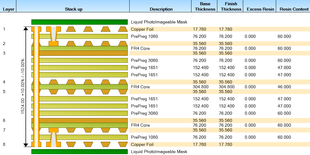
Model and document structure data and mesh/crosshatch geometry Speedstack PCB can be used in conjunction with the Si8000m field solver when modelling and documenting mesh/crosshatch ground. Structure data and mesh geometry can be readily shared between Speedstack and the field solver. The associated technical report also supports different materials on the same dielectric layer, improving the clarity of documentation between the stackup designer and fabricator. In addition, Speedstack PCB licence holders have full access to the stand alone Si8000m Quick Solver licence. Speedstack PCB is especially tailored for PCB fabricators and PCB brokers – anyone with a requirement to design or communicate controlled impedance PCB stackups. |
||
|
Speedstack PCB is ideal for you if:
By employing the link between the Si8000m field solver and Speedstack you can recalculate all the impedance values in a single pass in a fraction of the time taken traditionally. Speedstack provides data exchange with the companies below |
||
|
|
||
|
License options |
Speedstack PCB includes Speedstack and Si8000m |
Speedstack options |
| Request a Speedstack PCB evaluation | Feature request policy and process | Polarcare brochure |