|
|
|
|
|
|
Microstrip transmission line structures
Application Note AP122
|
|
Transmission line structures Today's high performance PCB traces are manufactured as transmission lines in microstrip or stripline construction. In this application note we look at several microstrip transmission line structures. A microstrip transmission line consists of a conductive trace of controlled width on a low-loss dielectric mounted on a conducting ground plane. The dielectric is usually made of glass-reinforced epoxy such as FR-4 or PTFE for very high frequencies. There are several configurations of PCB microstrip:
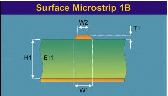
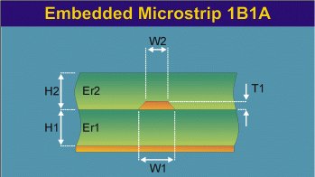
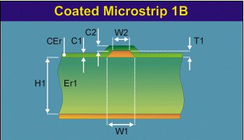
These structures are illustrated in the following diagrams. Single-ended Transmission Lines Single-ended microstrip transmission lines are probably the commonest way to connect two devices. In the single-ended transmission line case a single conductor connects the source of one device to the load of another device. The reference (ground) plane provides the signal return path. The impedance value is determined by the dimensions of the trace, the value of the board dielectric constant and thickness of the dielectric. Note that in the following diagrams the signal trace is actually trapezoidal in profile and width W refers to the trace width nearest the upper surface, W1 refers to the trace width nearest the lower surface. There are two basic configurations of microstrip, surface or exposed and embedded. |
|
|
|
The simplest configuration, the surface (or exposed) microstrip, shown left, consists of a signal line, the top and sides exposed to air, on the surface of a board of dielectric constant Er1 and referenced to a power or ground plane. Surface microstrip can be implemented by etching one surface of double-sided PCB material. |
|
The diagram shows the characteristic microstrip impedance attributes:
The effects of Er The value of Er, the dielectric constant of the board material, will be a significant component of the value of the characteristic impedance of the line. Designers therefore sometimes just specify the value of trace impedance and rely on the board manufacturers to control their processes to conform the impedance of the trace to the designer’s specification. Note that in the surface microstrip configuration the signal conductor is exposed to the air so the effective dielectric constant will be somewhere between 1 (that of air ) and about 4 (the Er of FR-4 substrate). This will also have an effect on the signal propagation velocity. Propagation velocity reduces (from the speed of light in air) as Er increases so the surface microstrip configuration provides the highest propagation velocity. However, the trade off is that radiation from the surface microstrip is higher than from embedded types. |
|
|
|
Embedded, or buried, microstrip is similar to the surface microstrip, however the signal line is embedded in a dielectric and located a known distance H1 from the reference plane. In this structure the dielectric is made up of two dielectric layers. |
|
|
Coated microstrip is similar to the surface version, however the signal line is covered by a solder mask. The solder mask coating can lower the impedance by up to a few ohms (depending on the type and thickness of the solder mask). |
Accurate calculation of the impedance of the coated microstrip structure requires that the designer supply values for the coating Er and thicknesses around the trace to the impedance calculator. The equations for characteristic impedance require very complex mathematics and impedances are usually calculated using field solving methods including boundary element analysis and are beyond the scope of this document. For further details of field solving methods and Polar's field solvers see Polar's Si8000m multiple dielectric controlled impedance field solver and Si9000e frequency dependent lossy line field solver. |
|