|
|
|
|
|
|
Designer's guide for Printed Circuit Board tolerances
Application Note AP521
|
|
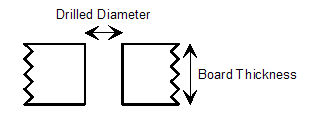
PCB materials PCBs are made from materials that will stretch, shrink, twist and bow. The most common material in general use is FR4. During the manufacturing process the laminates will be exposed to temperatures that will exceed their glass transition point (Tg) as well as many chemical processes. With this in mind, this note provides some general guidance on tolerances for PCBs. Board Thickness The standard thickness of a PCB is normally around 1.6mm; for a board of this thickness it is not unusual to have a thickness tolerance of ± 0.15mm. Note when calculating thickness that the supplier of the materials (for inner layer cores) quotes thickness values that do not include the copper weights. So for a 0.7mm core with double sided 1oz (35μm) copper the actual thickness will be 0.7mm + 0.035mm + 0.035mm — giving a total thickness of 0.77mm. Aspect Ratio In PCB fabrication the aspect ratio is the thickness of a PCB divided by the diameter size of a drilled hole — see Figure 1 below. It's importance relates to the plating process — plating solutions must flow through the hole efficiently in order to achieve acceptable copper plating. Hole sizes that are small compared with the board thickness can result in unsatisfactory plating.
Figure 1 Aspect ratio
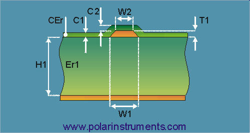
Anti-pad clearances in planes An anti-pad is a clearance in a copper plane that will allow a drilled hole to pass through it without making a connection. A good rule of thumb is to allow a least a 0.25mm (10 mil) annular ring clearance, so for a 0.5mm finished hole the anti-pad clearance should be 1mm. This may seem like a very large tolerance but it must be remembered that inner layers will stretch and shrink and drilled holes can wander. Controlled Impedance traces Due to etch factor, board thickness variances and dielectric (Er) values that are variable, it is necessary to allow a reasonable tolerance to be applied to the controlled impedance traces. For example, for a simple coated microstrip with a target impedance of 75Ω it would not be unusual to specify a tolerance of ± 5%; typically, though, impedance is more often specified with a tolerance of ± 10%. Remember – the tighter the tolerance the more the PCB will cost. Consider Figure 2 below:
Figure 2
Note: for the dielectric constants for the solder mask a good starting point is to use an Er of 3.5 to 4 None of the factors above can be absolutely controlled so variances between calculated and measured impedances will occur. These are just a few examples of the tolerances in PCB fabrication; if in doubt talk to the manufacturer of your PCBs – they will be able to provide you their in house standard tolerances. If the specified tolerances are too tight it may become impossible to fabricate a board or if it can be produced it will probably incur higher costs to accommodate a higher scrap ratio. Polar Speedstack products Share & design accurate stackup specification drawings with Speedstack Share & design accurate impedance controlled stackup specification drawings with Speedstack PCB Share & design accurate insertion loss controlled stackup specification drawings with Speedstack Si Share & design accurate HDI stackup specification drawings with Speedstack HDI Share & design accurate Rigid-Flex stackup specification drawings with Speedstack Flex |